
Intel Reveals 10nm Sunny Cove Core, a New Core Roadmap, and Teases Ice Lake Chips
Introducing Sunny Cove
Ronak Singhal, Intel Chief Core Architect presented Intel’s next-generation big core microarchitecture – Sunny Cove. The core will be found in future Ice Lake chips among other products. Note that Sunny Cove will be used for both the server chips, the usual client chips, and a number of other products. Sunny Cove was designed by Intel’s Israel Development Center (IDC), Intel’s talent stronghold.
Front End
We want to point out that the modifications done to the front end of Sunny Cove were intentionally not disclosed during Architecture Day. Ronak disclosed just one detail which is that the micro-operation cache was made bigger. The rest of the design will be discussed at a future Architecture Day in 2019.
Back End
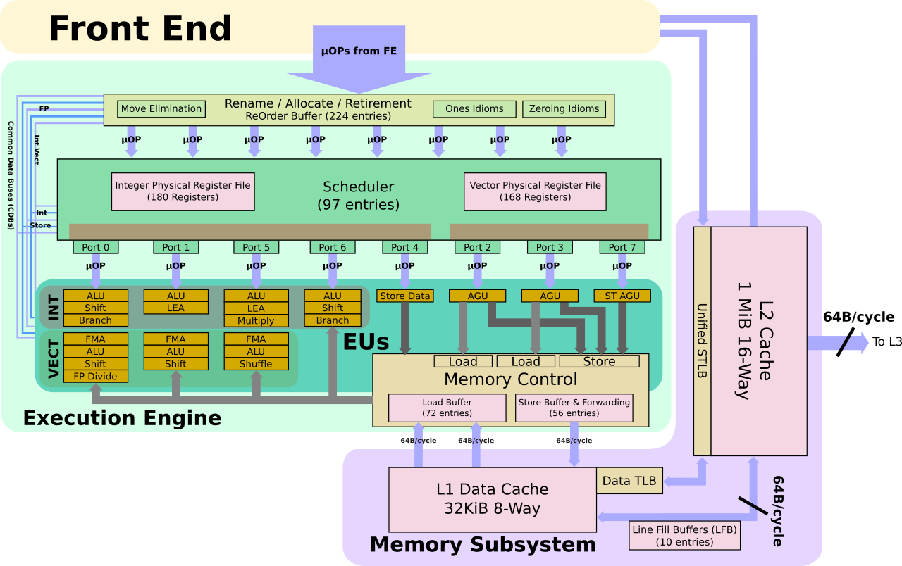
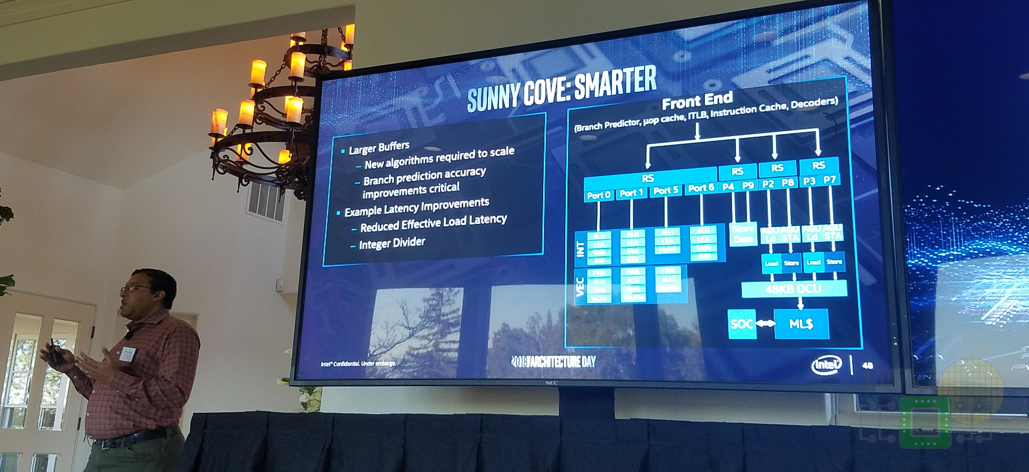
The focus of Sunny Cove initial disclosure is about the OoO portion of the core and the execution units. Intel believes Sunny Cove delivers a significant IPC increase. The execution engine on Sunny Cove has evolved quite a bit from Skylake. In order to find more sets of independent instructions to extract more parallelism in order to execute them simultaneously, the buffers have to increase. To that end, Intel says it has increased all the major buffers in the core. This includes the load and store buffers, the ROB, and the scheduler. No precise numbers were given out but Ronak noted all of those buffers grew substantially from Skylake.
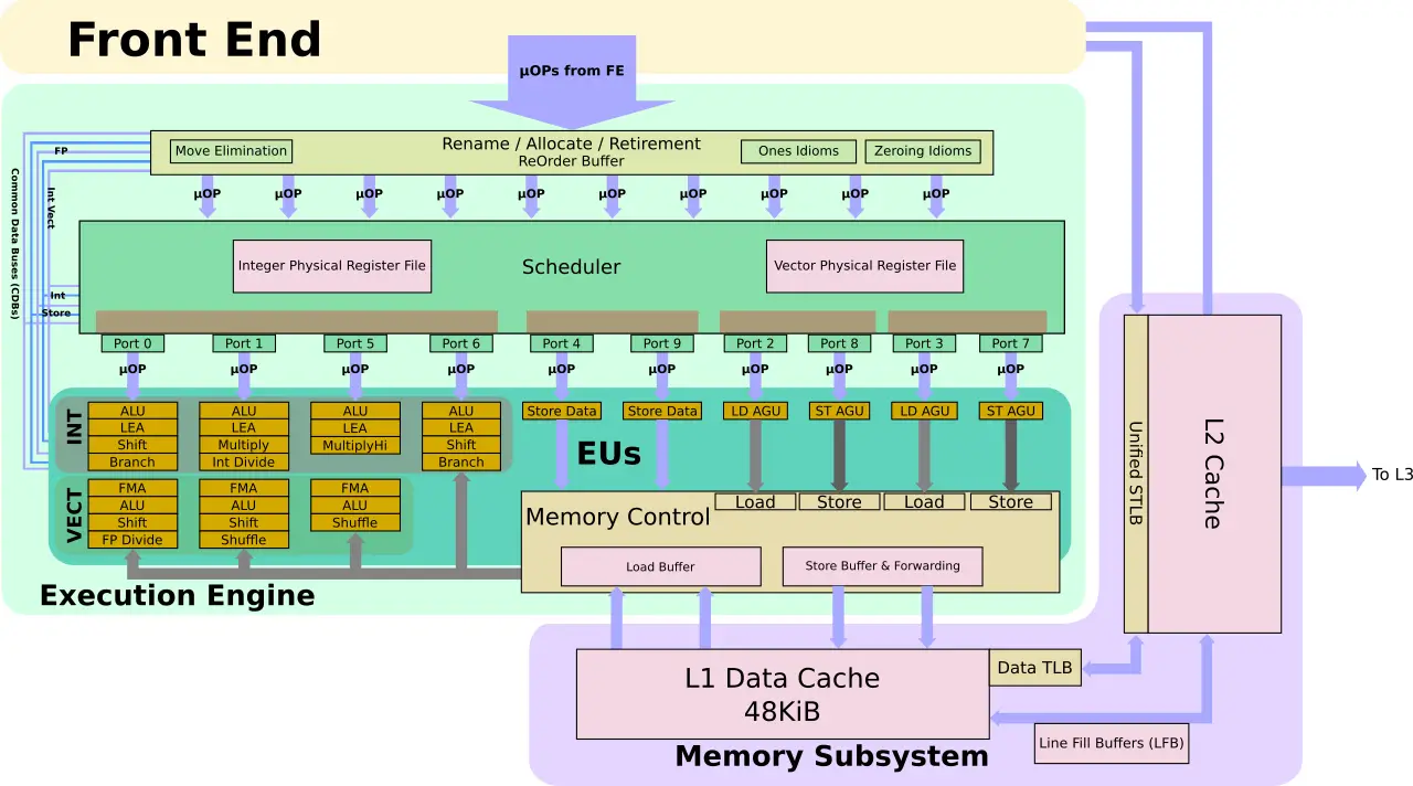
In addition to the larger buffers, the core is now much wider. Sunny Cove can now allocate (i.e., rename) five instructions each cycle. The rename is where the mapping from architectural to physical registers takes place. In Sunny Cove, it means five fused micro-operations can be renamed each cycle. This means up to ten uops may be sent downstream. By the way, we asked if this meant the commit was also increased to match the renamer (currently it’s 4). We couldn’t get an answer on that just yet so, at least for now, we will assume it has not changed.
| Skylake |
|---|
 |
| Sunny Cove |
 |

Execution Units
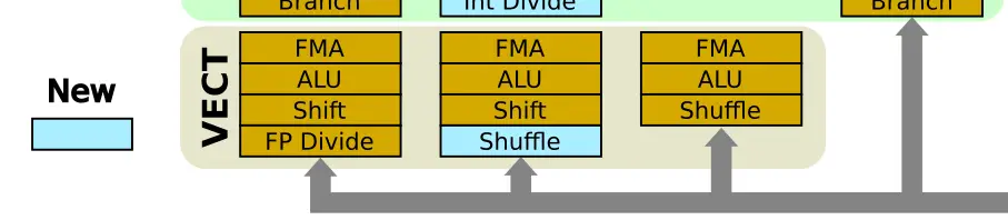
The scheduler on Sunny Cove is really wide – 25% wider than Skylake. Up to 10 operations may be dispatched each cycle. All the added execution units are part of the memory subsystem which is discussed in the next section. On the arithmetic side of the execution engine, the four workhorse ports were augmented with more functionality. On the vector side, Sunny Cove retains the three FMAs and ALUs. One of the key changes here is the addition of a new shuffle unit on Port 1 for moving data within a register. You may have noticed we didn’t mention the width of those units. The reason is simple. That hasn’t been disclosed yet. One possibility is that all three units are now 512-bit wide. Alternatively, Port 0 and Port 1 might still be used like in Skylake. Whatever the case may be, the second shuffle unit is a much-welcomed addition, even if they two units are not symmetrical. By the way, since Sunny Cove goes into both the client and server microprocessors, it’s entirely possible we will see different widths between the two.
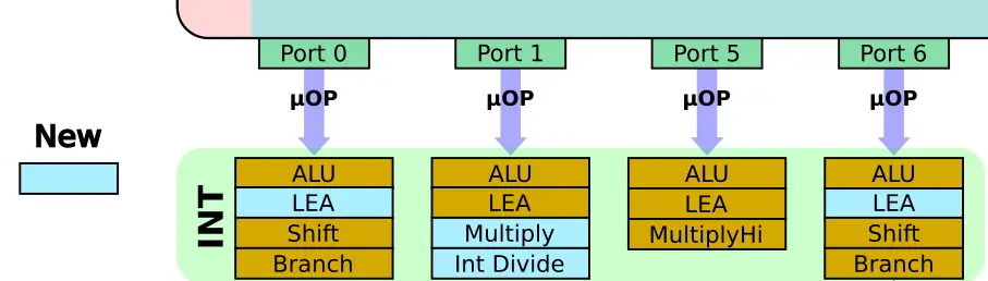
On the integer side, Sunny Cove doubles down on LEAs, a very common operation for computing addresses although it’s also commonly used for doing various generic math operations. There are now four LEA units, one on each port. This actually seems a bit excessive. Generally, there are not as many such sequational operations to extract parallelism from. It’s also possible this was done to help with hyperthreaded workloads. Sunny Cove added a new integer divide as well as a multiply hi unit. By the way, the new divide unit was actually added in Cannon Lake.
Memory Subsystem
Sunny Cove has had a number of major changes to the memory subsystem. Some are a first in over 2 decades! Dating back to the Core microarchitecture and even the Modified Pentium M (Yonah). One of those changes is the L1 data cache size which has increased in capacity by 50% to 48 KiB. Presumably, this also means they have gone with 12-way. The implications of this are interesting in a number of ways, worthy of a whole article just on that but beyond the scope of this article. The L2 cache has also been increased. Note that like Skylake, the L2 size will differ between the server and client chips. Exact sizes were not given but Ronak stated that in both cases, the cache is larger. The STLB has also been increased in tandem with the L2 changes.
All the cache changes bring us to the AGUs. Here we are seeing changes larger than what we saw with Haswell. In Skylake (inherited from Haswell), there are two generic AGUs and one Store AGU. In other words, there were two units for handling address generations for both loads and stores and an additional unit for address generation for stores only. This meant Skylake could sustain two loads and one store each cycle.
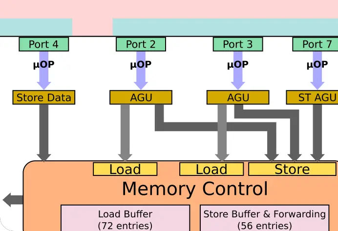
In Sunny Cove, all the ports were reworked. The generic AGUs are gone. Each port is now a dedicated AGU, capable of handling either one load or one store. In general, stores requires two operations – one to generate the address and one to write the data. Here, Intel added a fourth port (Port 8) for handling another store. Complementing the new store AGU execution unit is a second store data port (Port 9). This means the new design is capable of sustaining two loads and two stores each cycle. Skylake was capable of 128 simultaneous memory operations in-flight and given those buffers grew significantly in Sunny Cove, we could see this number approaching 200.
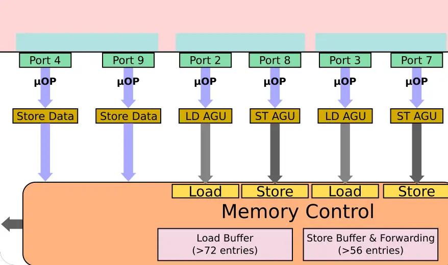
The new design is slightly more balanced but actually, there are some interesting peculiarities here. A typical program exhibits a ratio of roughly two loads for every store. The extent of the benefits of adding a whole second store is unclear especially since there is a lot of new logic and a lot of complexity involved here. In many ways, this looks to improve multithreaded workloads. Either way, we will have to wait for benchmarks to clear this up.
New Algorithms
One of the more interesting aspects of Sunny Cove is power efficiency which is a very important optimization vector for Intel. Blindly increasing all the buffers doesn’t automatically improves performance and it certainly doesn’t improve the power efficiency of the core. To that end, Ronak stated that part of their secret sauce in Sunny Cove is new hardware algorithms that enable higher power efficiency while increasing the buffer sizes and increasing the OoO execution window. One example that was given is the reduction of “effective load latency” in Sunny Cove. What this means is that despite no changes to any particular cache level, the effective latency is improved through better algorithms that can accelerate load operations under various conditions. It goes without saying that along with new algorithms are improvements to the branch predictor accuracy as well.
Specialized Workloads Enhancements
Along with the classical IPC improvements, Sunny Cove adds a whole slew of new ISA extensions for accelerating all kinds of workloads, especially cryptography and compression.
- Crypto Acceleration, Special Math
- Big number arithmetic
- Vector AES
- Vector Carryless Multiply
- Galois Field
- SHA
- Special SIMD, Compression/Decompression
- VBMI (permute, shifts)
- VBMI2 (expand, compress, shifts)
- BITALG (population count, bit shuffle)
Miscellaneous Capabilities
The new core adds few new security and memory enhancements. One of the interesting changes is the new support for larger memory capacity. Intel is moving from a 4-level paging structure to a 5-level paging structure. Sunny Cove is moving to a significantly larger address space – one with a virtual address space of up to 57 bits and a physical address space of up to 52 bits. You are now looking at the ability to have up to 4 PiB of memory on a single system with up to 128 PiB of virtual address space.
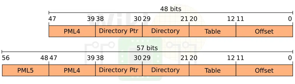
The new addresses are now 57-bit canonical meaning the remaining, non-participating, high-order bits (i.e., 63:57) are copies of bit 56.
On the security enhancements side, Sunny Cove will have support for their Total Memory Encryption (TME) extension as well as the multi-key sub-extension. In addition to that, Intel added User Mode Instruction Prevention (UMIP) support to Sunny Cove as well. Previously, UMIP started shipping with Goldmont Plus on their small core microarchitecture. UMIP is a simple security feature that simply prevents the execution of certain legacy instructions (e.g., Store Global/Interrupt/Local Descriptor Table).
–
Spotted an error? Help us fix it! Simply select the problematic text and press Ctrl+Enter to notify us.
–