
ISSCC 2018: Intel’s Self-Powered Intelligent IoT Edge Mote
Memory
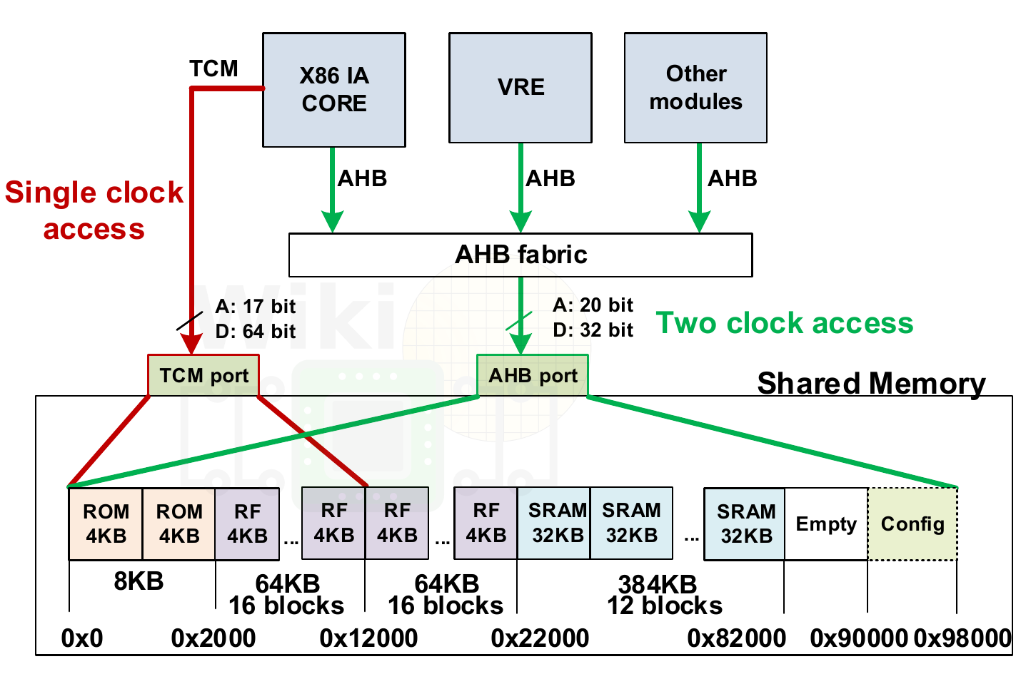
The SoC has a unified memory consisting of 8 KiB of ROM (2 banks of 2 KiB each), a 64 KiB register file array of 16 banks and 12 banks of 32 KiB for a total of 384 KiB of SRAM. The unified tightly coupled memory (TCM) consists of the ROM and register file and is connected directly to the x86 core for fast boot and better performance by providing single clock access. Because the 384 KiB of SRAM is mainly used for the image bytes, it’s not accessible through the TCM and is generally clock gated entirely when the CNN/Image states are not in operation. While the x86 core has a dedicate fast TCM port, it, along with all other modules, can access the full memory via the AMBA High-performance Bus (AHB). This operation is slightly slower, requiring two clock cycles to access.
It’s worth noting that the reason the memory is designed in blocks of 4 KiB is because the system power management is capable of performing fine-grained power gating down to a granularity of single 4 KiB banks. The system turns memory blocks on and off for various states depending on the usage.
Crypto Engine
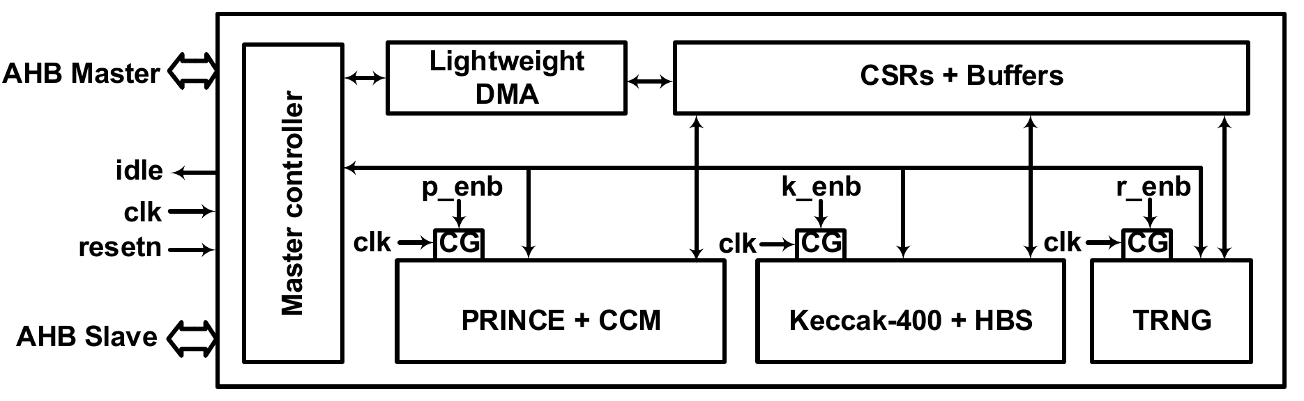
As was shown by MIT’s processor in the same conference session, a hardware crypto engine is crucial for reducing memory and power consumption. For this SoC Intel designed a low-power crypto engine in order to facilitate secure boot and secure wireless communication. Secure boot is based on secure XMSS public key signature verification. On boot, the crypto-DMA brings the boot-image from the external flash, validates the signature, and loads it into memory. This is done through lightweight crypto DMA logic and the accompanying Keccak-400 Hash block. For secure communication, there is a lightweight PRINCE block-cipher (128-bit Key) with CCM authenticated/encryption engine with an all-digital true random number generator (TRNG). This is used to preserve confidentiality and integrity of sensor and image data during local storage as well as transportation.
Visual & CNN
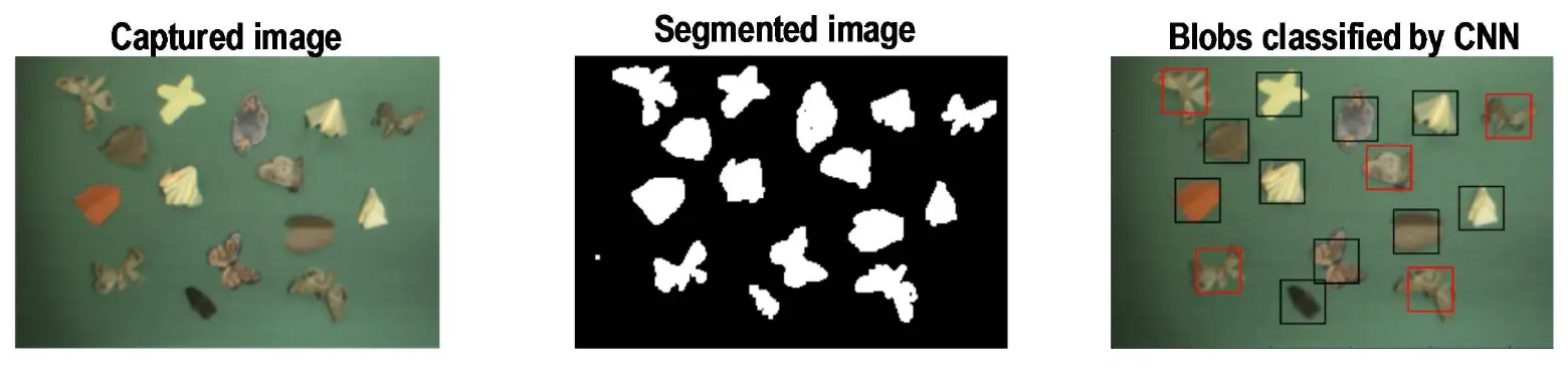
The visual subsystem is responsible for the image capturing and processing. Captured images undergo color conversion and scaling followed by color-based segmentation. This is mainly done to eliminate the background pixels through binarization, clustering, and color-based thresholds. For example, a histogram-based scheme applied to a grayscale conversion is done followed by thresholding to segment the image. Possible moth candidates are identified and segmented while a hue-based segmentation scheme is used to lower the number of blobs generated. Fewer blobs mean fewer evaluations through the recognition engine is required which ultimately translates to less power and reduced memory footprint.
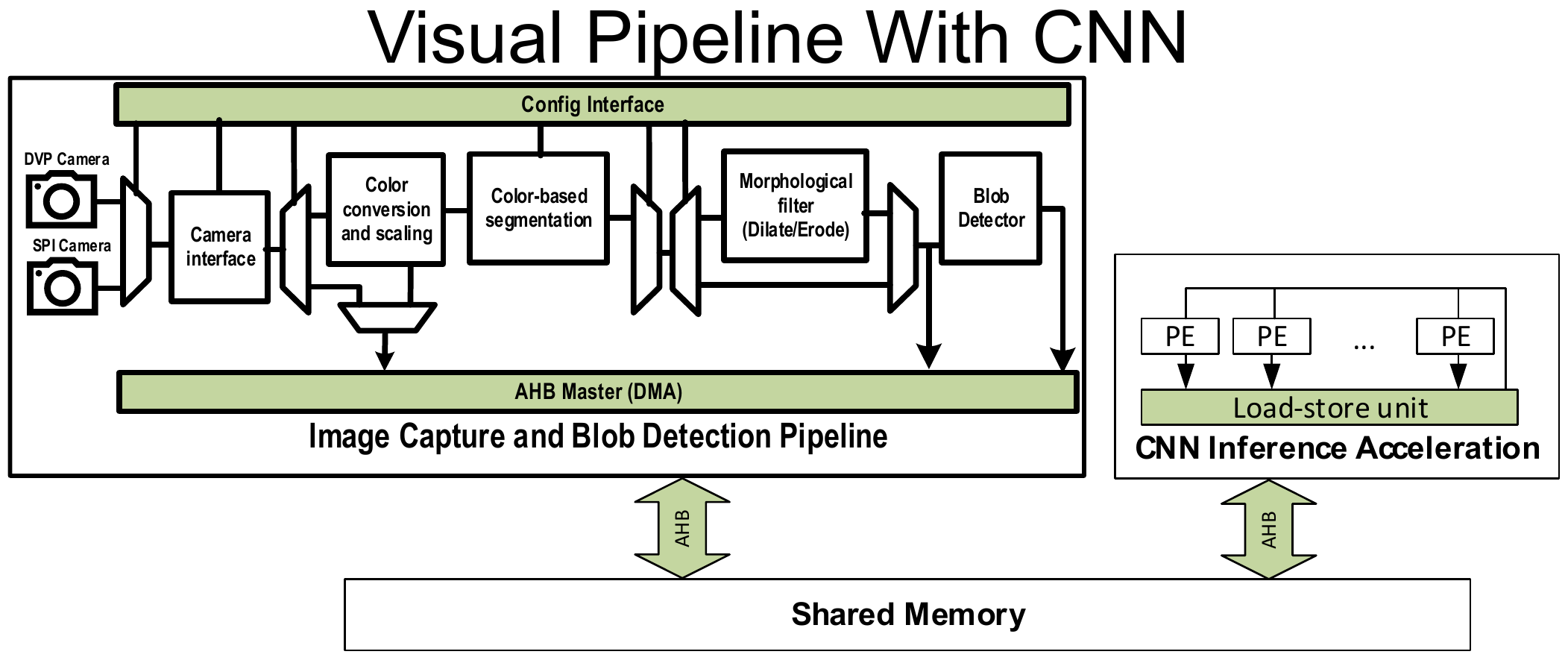
Note that the entire blob detection pipeline operates on the fly as the images are captured. Blobs and the original image are stored in the shared memory. The CNN weights are brought layer by layer from the external flash. Only 8b resolution is supported by the accelerator. The detect blobs from earlier are then fed into the pre-trained CNN classification accelerator for moth recognition.
In the example test below, the captured image is segmented and the background is removed. The image is then passed through a dilation filter to reveal the detected blobs in the white areas. Individual blobs are then classified by CNN with red rectangles marking identified moths.
x86 Core
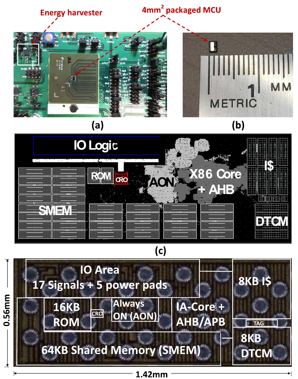
This SoC incorporates a near-threshold voltage (NTV) x86 core Intel described earlier last year. Fabricated on their 14nm process, the core implements Intel’s IA32 ISA, and is capable of operating at 500 KHz to 300 MHz at 17.18pJ/cycle at roughly 17μW/MHz. Interestingly, Intel noted that this is a Quark derivative (similar to Lakemont). This is possibly the same core which can also be found in the Loihi research chip.
The chip described last year (shown below) was a full energy-harvesting stacked wireless sensor node. In that work, the chip was fabricated on Intel’s 14nm (looks to be 3rd generation ++ with 84nm poly pitch instead) with nine metal interconnect layers. The die area was 0.79 mm² (0.56 mm × 1.42 mm), consisting of 213,000 cells. For this edge mote compute SoC, much of the guts was taken out including the I/O and memory which reduced the overall core size considerably.
The Die
The final SoC is a 12-million transistor chip manufactured on Intel’s 14nm process on a 2.5mm x 2.5mm die. The x86 host processor consists of 307,000 gates, while the visual subsystem makes up another 1,040,000. There are around 8 million transistors used for logic with another 3.6 million used for memory.
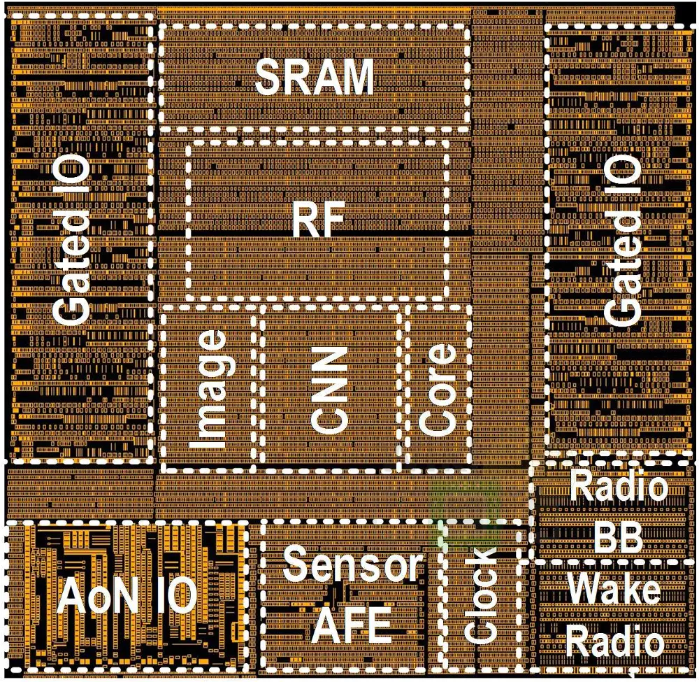
The breakdown for each of the major blocks is shown below.
| Logic Gate Count | |
|---|---|
| Block | Logic Gate Count |
| AFE wrapper | 24K |
| Image | 440K |
| Wake Radio BB | 278K |
| CNN | 600K |
| Core | 307K |
| Crypto | 70K |
| PMU-Clock | 50K |
| Rest | 290K |
Final Device
The chip was demonstrated to work at 200 KHz at 0.4 V to 950 MHz at 0.85 V with 80μW-to-17mW power consumption. Operating at near-threshold voltage, the SoC is capable of 6.2 pJ/cycle at 0.5 V and 100 MHz. This is a total platform power which consists of 16-24mW for the visual subsystem and image processing, 1-7 mW from the camera during capture, 14 mW and 1-3 mW in the gated I/O and logic blocks, and 100-200 μW in the embedded SRAM.
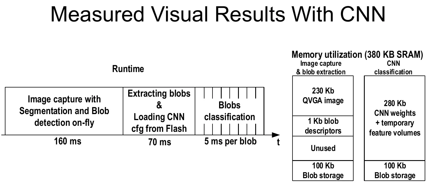
The final prototype can achieve 56ms secure boot and demonstrated functional image capturing and processing capabilities. The prototype does 160ms image capture with segmentation and blob detection as well as 70ms blob extraction and CNN setup and configuration, and finally 5ms classification per blob.

–
Spotted an error? Help us fix it! Simply select the problematic text and press Ctrl+Enter to notify us.
–