
VLSI 2018: Samsung’s 11nm nodelet, 11LPP
 As the industry continues to face growing challenges with device scaling, manufacturers look for other ways to provide value with less uncertainty and risk. One such example is Samsung’s introduction of the 11nm “11LPP” nodelet. At the 2018 Symposia on VLSI Technology and Circuits that was held last week, Samsung provided us with some more information about their improved process.
A Mix of Old and New
Samsung’s 11nm bulk FinFET process uses the foundry 14nm devices in conjunction with a new optional 10nm BEOL. By leveraging their existing technology Samsung hoped to offer a better process while yield ramping faster than most recent nodes. At the conference, they reported sub-1% gap to their current 14nm production.
PPAC – Area
A number of different standard cells were introduced for their 14nm process: their original 9T 14LPE standard cell (the same as 14LPP HD cell) and two high-performance cells – 9T (HP) and 10.5T (UHP). Note that two high-performance cells use a relaxed poly pitch of 84nm.
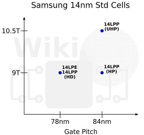
It’s worth pointing out that Intel’s highest performance transistors (14nm++) also uses this very poly pitch, albeit they are quite a bit denser.

For this node, Samsung added a second option that uses their 14nm devices and the shrunken metallization stack from their 10nm process. The combination of those two technologies allowed Samsung to introduce a new ultra-high-density (UHD) standard cell for low-power applications. This cell has a height of 6.75T, a reduction of 25% from the 9T in their 14nm (14LPE, 14LPP) nodes. This library is positioned for cost-sensitive/power-sensitive applications.

Existing IPs and designs do not have to use the new cells but can benefit from the other process optimizations that were done (e.g., power reduction).
| Samsung 14nm and 11nm nodes | |||
|---|---|---|---|
| Node | 14LPP | 11LPP | |
| PP | 78nm | 78nm | 84nm |
| Height | 9T | 9T | 6.75T |
| Cell Area | 1.00 | 1.00 | 0.81 |
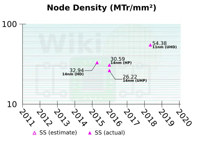
At 6.75T, Samsung’s 11nm ultra-high-density cells are actually comparable in density to the 10nm node but fall short in terms of performance.
Fin Profile
The aspect ratio and profile of the fins have been improved. Compared to 14LPP fins, 11LPP fins are now taller and narrower. In fact, it’s quite clear that the fin was adjusted in a similar manner to the improvements that were done to with their 10nm fins.
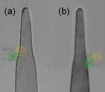
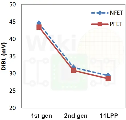
Note that the images above might not be to the same scale, therefore pixel-counting the dimensions of the improved fins is not possible. The profile changes were done to improve the short channel behavior and support shorter Lg. To that end, Samsung reports sub 30mV measurements, a modest improvement over 14LPP.
Samsung reported upgrading the multi-eWF gate stack in order to enable ultra-low-power (ULP) HVT transistors, however, they refused to disclose much more beyond that (even when we tried to ask more questions after the session). They also performed some optimization in the source-drain epitaxy process. Though they did not go into any details, improving the dopant density can result in a modest reduction in resistance.
PPAC – Power, Performance
Compared to first-generation (14LPE), 11LPP improved by 25% in ring oscillator AC frequency at same IDDQ or conversely, Samsung reports 42% power reduction. When compared to second-generation, 11LPP provides roughly 14% higher frequency at the same IDDQ.
| Device Power | |||
|---|---|---|---|
| Node | 14LPP | 11LPP | |
| PP | 78nm | 78nm | 84nm |
| Height | 9T | 9T | 6.75T |
| Power | 1.00 | 0.86 | 0.65 |
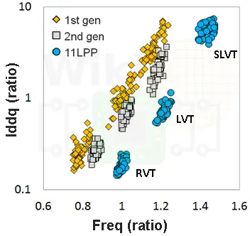
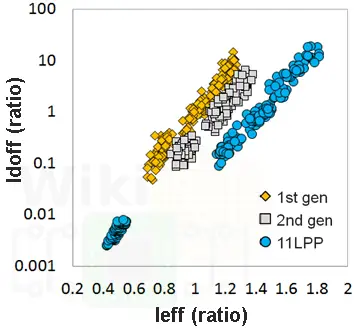
One of the new additions to 11LPP is the introduction of a new optional ultra-low power (ULP) device that achieves ~10pA/µm Idoff at 0.7 volts, comparable numbers to what Intel reported with their 14nm ULP devices back at VLSI 2015. The standard SLVT (Super Low Vt) device has significantly improved as well. For those devices, Samsungs reports reaching 20% higher frequencies. Compared to second-generation 14nm (14LPP), those devices have 17% and 21% higher DC performance for nFET and pFET respectively.
| 11LPP DC Performance Improvements Over 14LPP | |
|---|---|
| nFET | pFET |
 17% Higher DC Performance |
 21% Higher DC Performance |
| (VLSI 2018, Samsung) | |
PPAC – Cost
By leveraging existing 14nm and 10nm technologies, 11LPP is ramping to Samsung’s 14nm yield levels very quickly. For those who seek a less expensive upgrade path (at least compared to moving to a new node), the process itself offers a compelling upgrade from 14LPP for either its extra density and lower power or performance with relative ease – 11LPP FEOL is design-rule-compatible with 14LPP. Some minor changes were necessary for the BEOL 1x layers where the tighter 48nm M2 was introduced. It’s also worth noting that with a 48nm pitch, Samsung had to move to LELELE (LE3) which does add some complexity but they did note that overall cost is very similar to their 14LPP process. Both Samsung and ARM expect 11LPP to become long-lived node which is why they have expanded their platform offering to additional markets such as automotive and Internet of Things (IoT) sectors.
–
Spotted an error? Help us fix it! Simply select the problematic text and press Ctrl+Enter to notify us.
–