
GlobalFoundries 14HP process, a marriage of two technologies
As IBM starts shipping their latest and greatest server microprocessors, it’s a good time to take a look at the underlying fabrication process. Fortunately, over the last few months we have had the opportunity to attend a number of conferences where enough aspects of the process was revealed to build complete picture.
This is GlobalFoundries 14HP Now
In October 2014 it was announced that IBM has agreed to pay Globalfoundries $1.5 billion to take over their unprofitable foundry. In addition, Globalfoundries was to remain IBM’s sole provider for the next decade. By that time, design rules for IBM’s 14nm process were already set and shortly after IBM presented their 14HP technology at IEDM 2014. Three years after the original fab deal, in September 2017, GF announced 14HP was finally ramping up production. At the time there were a few murky details in the official press release that piqued our interest. In particular, there was one small statement describing the metal stack which differs from what was described back in 2014 and of course Tom Caulfield (SVP and GM, Fab 8) quote that claimed 14HP “leverages the proven 14nm FinFET high-volume experience of our Fab 8 facility”.
We now know why.
At a recent conference IBM explained that GF 14HP had indeed changed from their original 14HP design. In particular, GF 14HP combines IBM-developed SOI front-end-of-line (FEOL) with GF’s middle-of-line (MOL) and back-end-of-line (BEOL) borrowed from their 14nm bulk process.
Overview
14nm High Performance (14HP) process has been optimized for different vectors than the low-power-optimized processes developed by companies such as Samsung and TSMC. In order to avoid any confusion, we want to point out that 14HP is very different from GlobalFoundries standard bulk CMOS process (e.g., 14LPP) used by products such as AMD’s Zen.
The main features of 14HP are:
- FinFET on a silicon-on-insulator substrate
- Deep-trench capacitors
- Support >5GHz clock
- Support >1.1V operations
- High-κ metal gate
- Double patterning for the critical patterning layers
- Multi-workfunction (multi-WF) Vts
- 17 metal layers BEOL
- BEOL stack designed to maximize manufacturability of very large dies (≥ 700mm²)
- Unique DT eDRAM
- Full suite of analog devices supported
Key Features
Below is a few key transistor geometries. Note that the comparison is against IBM’s 22nm, not GlobalFoundries 20nm.
| Key 22nm and 14nm Geometries | |||
|---|---|---|---|
| Feature | 22nm | 14nm | Scaling |
| Fin Pitch | N/A | 42 nm | N/A |
| Gate Pitch | 100 nm | 80 nm | 0.80x |
| Minimum Metal | 80 nm | 64 nm | 0.80x |
This is IBM’s first generation of FinFET and as far as we know it’s also the first and currently only FinFET on a silicon-on-insulator (SOI) substrate process. What this means is that they use an insulating substrate instead of the standard bulk substrate, which, while more expensive is promised to simplify fabrication and profile control of the fins and isolation.
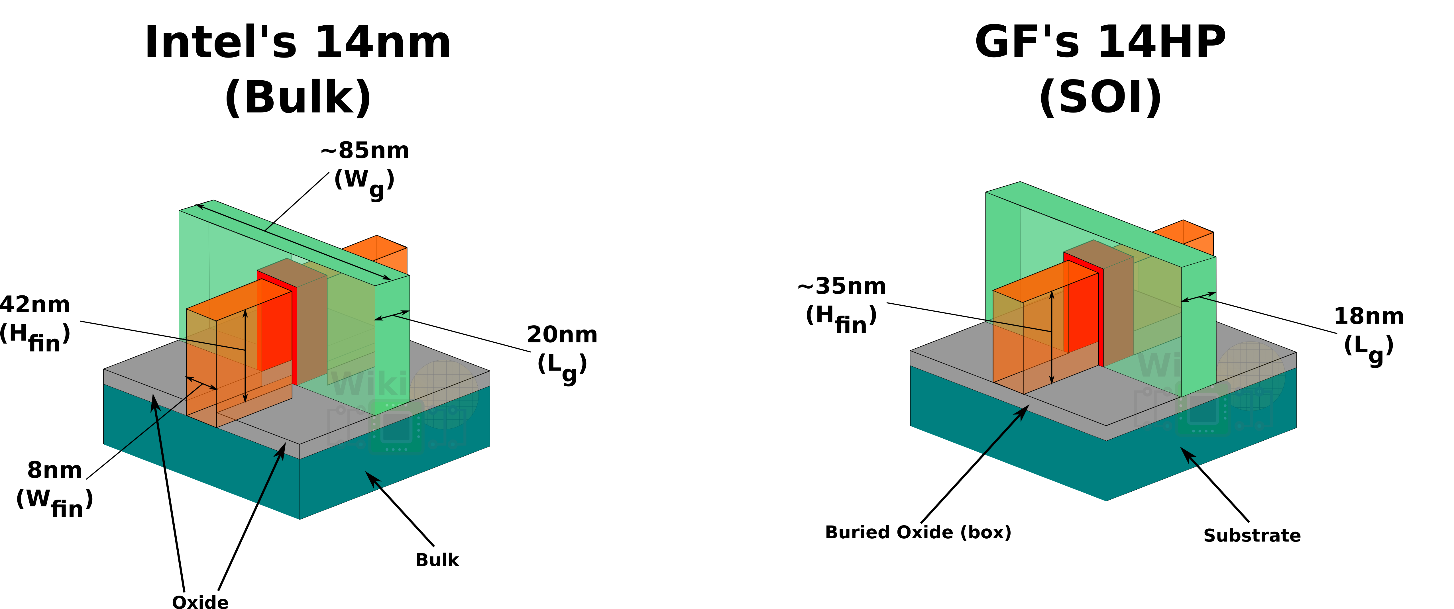
Since we couldn’t confirm the fin width, it’s rather hard to estimate the gate width.
Density Improvement
Since 14HP is already shipping and IBM has been pretty forthcoming when it comes to their dies stats we don’t need to use a theoretical metric such as MTr/mm² to estimate the density improvement. Using IBM’s actual numbers for their z13 and z14 chips we can measure their effective improvements from real products.
| Die Stats | ||||
|---|---|---|---|---|
| System | Process | Transistors | Die | Effective Density |
| z13 | 22nm SOI | 3.99 Billion | 679 mm² | 5.88 MTr/mm² |
| z14 | 14nm SOI | 6.1 Billion | 696 mm² | 8.76 MTr/mm² |
| POWER8 | 22nm SOI | 4.2 Billion | 649 mm² | 6.32 MTr/mm² |
| POWER9 | 14nm SOI | 8 Billion | 695 mm² | 11.51 MTr/mm² |
For both Z and POWER the effective density has increased by 1.5x-1.8x demonstrating a solid density improvement over the 22nm node. It’s worth noting that real chip transistor density is considerably lower than the theoretical max but that’s ok given how well the density has improved in practice.
–
Spotted an error? Help us fix it! Simply select the problematic text and press Ctrl+Enter to notify us.
–