
GlobalFoundries 14HP process, a marriage of two technologies
Deep Trench (DT) Structures
Among the many unique features of this process is IBM’s continual use of dense deep-trench structures for various applications such as their dense DT eDRAM as well as decoupling capacitors. IBM has been using DT structures for four generations now (since their 45nm node) and have since gained significant know-how working with DT structures and testing them. DT eDRAM gives them a competitive advantage over SRAM as cache memory due to the significant density advantage since we have a single transistor and a single bit storage capacitor.

DTs are traditionally created by etching an opening in the hardmask or alike layer. Using a technique such as reactive-ion etching you form a deep trench. The Deep trench extends through the top silicon, through the oxide layer and into the base substrate. You then remove the hardmask and a thin high-k dielectric (like HfO2) is deposited and grown in the trench. After that, the low-resistivity titanium nitride (TiN) conformal layer is added. Finally a liner is applied after which the trench is filled with the highly-doped (probably arsenic-doped silica glass (ASG)), n-type polycrystalline silicon. A rough diagram is shown below.
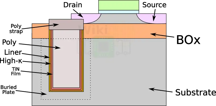
The poly with all the other layers go up to and into the BOx but stay fully within the BOx. A poly strap (i.e., the interface between the poly and the drain) is then formed on the high-k dielectric layer, metal layer, and poly layer. Below is what the final structure looks like on IBM’s 45nm SOI process.
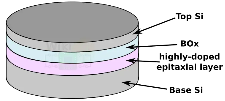
We should point out that starting with their 22nm node, IBM made a substrate change where they use an N+ epitaxially pre-doped wafer instead of the previously used cell plating technique. Since this eliminates the need for the sidewall nitride spacer they have always used previously in order to protect the BOx during the interim processes, this change effectively managed to extract additional density from the denser packing of the trenches.
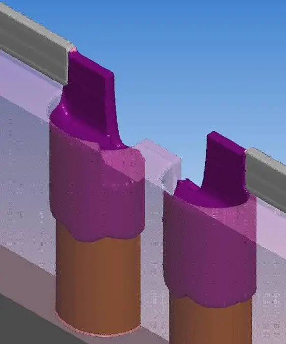
In this 14nm process IBM switched to a FinFET from a planar transistor which introduces a new set of challenges since they now have to connect to a thin fin meaning the strap size is also reduced meaning resistivity becomes a more profound problem. On the FinFET, the strap is formed where the base of the fin lands at deep trench. There, the fin switches from mono-Si to poly-Si which forms the connection to the DT capacitor. The strap area is then highly doped during the S/D epitaxial Si deposition process in order to ensure a good connection with minimum resistance. In addition to the resistance, the significant reduction in the strap’s cross-sectional area due to the fin also implies we should expect regression in the RC performance. However IBM claimed that by switching to FinFET and through various other enhancements, their 14nm eDRAM saw a reduction in access time allowing it to be utilized in their L2 caches where desired.
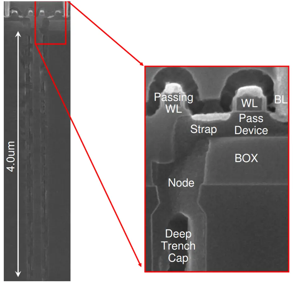
Below is a cross-sectional SEM shot of the entire stack from the 40x power rails at the very top to the deep trench capacitors under the devices.
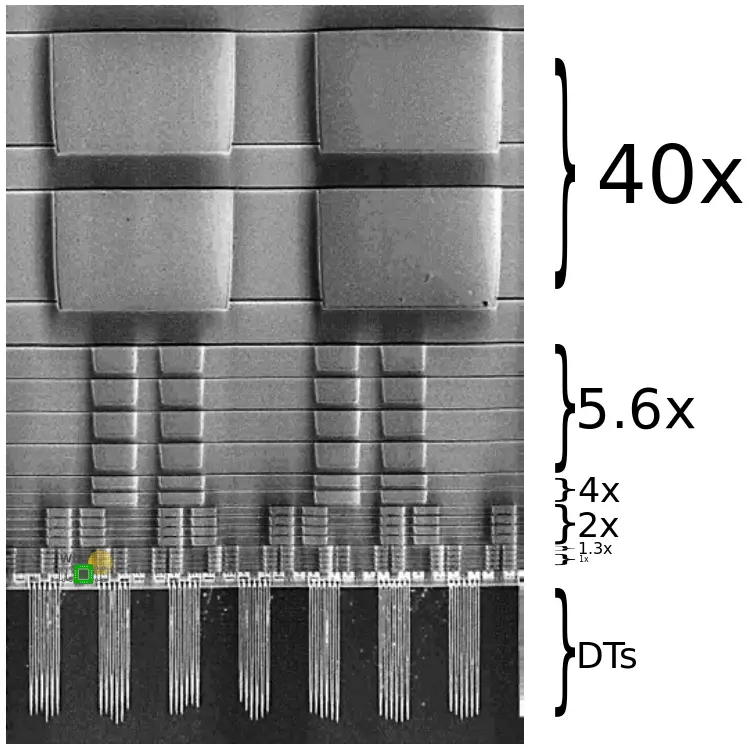
Those trenches do go fairly deep, as much as 3µm.
DT eDRAM
The entire process described leads to the final product – the deep trench embedded DRAM. GlobalFoundries 14HP boasts an ultra-dense 0.0174 µm² eDRAM bitcell, almost 3x the densest 14nm SRAM reported which was 0.0499 µm² by Intel. Though it’s worth pointing out that Intel has their own eDRAM process albeit it’s an entirely different capacitor-over-bitline (COB) architecture embedded inside the interconnect layers.
| IBM’s eDRAM | ||
|---|---|---|
| Node | Area | Scaling |
| 65 nm (not in prod) | 0.127 µm² | N/A |
| 45 nm | 0.067 µm² | 0.53x |
| 32 nm | 0.039 µm² | 0.58x |
| 22 nm | 0.026 µm² | 0.67x |
| 14 nm | 0.0174 µm² | 0.67x |
–
Spotted an error? Help us fix it! Simply select the problematic text and press Ctrl+Enter to notify us.
–