
GlobalFoundries 14HP process, a marriage of two technologies
Benefits
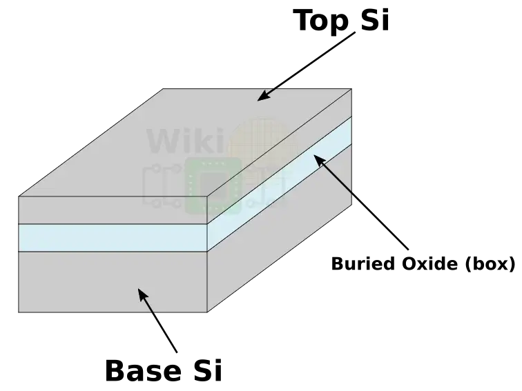
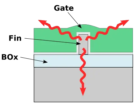
Earlier we mentioned some claims regarding the SOI process. In a standard bulk FinFET such a what Intel has been using for their 22nm, 14nm, and 10nm processes, you etch the tall fins first and then you fill it with an oxide. You then recess the oxide layer back down to expose the fin at the desired height. In the case of this SOI process, you start with a top and base silicon layers and in between you have a buried oxide (BOx) layer.
You then simply etch the top Si layer in order to expose your fins.
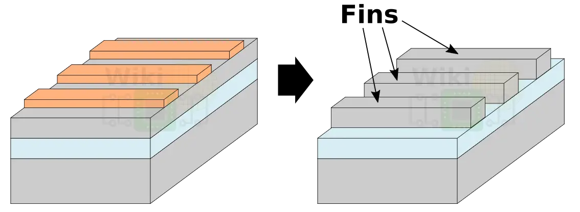
This is where some of the benefits become obvious. Since you are etching the top layer to expose the fin, the fin definition is predefined by the height of the top Si layer.
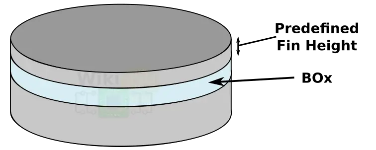
Since the fin height is predefined by the thickness of the silicon, you get fins with very unified height; that is, the variations in fin height compared to bulk is very low.
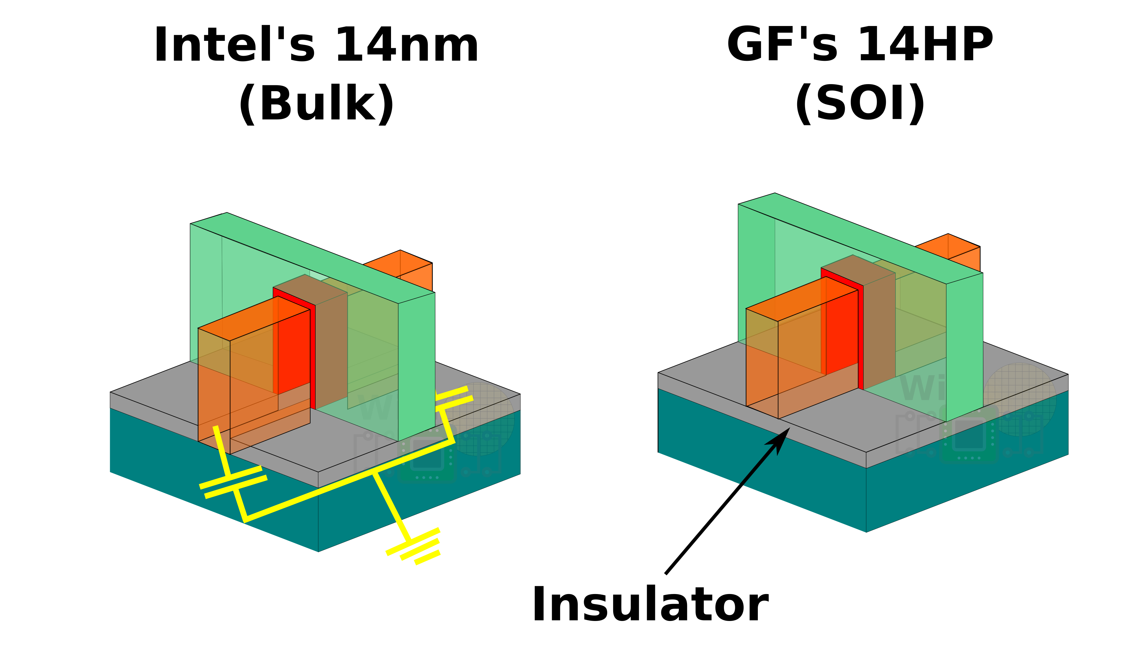
The other argument IBM makes is that this process significantly minimizes the parasitic capacitance at the base of the fin. Every material has capacitance which is the ability to store a little bit of electrical charge. When you switch a transistor, you have to first charge any internal capacitance it may have before it starts to conduct electricity. In fact, charging and discharging takes a good chunk of time compared to the actual switching time. This undesired internal capacitance causes the transistors to deviate from their ideal behavior, among other things by also slowing them down. It is therefore advantageous to reduce the capacitance as much as possible.
A major source of parasitic capacitance that SOI significantly reduces is the capacitance at the source and drain junction at the base of the fin. With the thin insolation layer now placed between the device and the substrate this capacitance is reduced.
Drawbacks
As usual, nothing comes for free and there are of course a number of disadvantages to this process. The biggest one is that bulk substrate is much cheaper than an SOI substrate. In theory if a company such Intel was to adopt it for their high-volume process, this overhead cost can be absorbed, but IBM has no such volume and this does directly translates to higher manufacturing cost for them (although they did ship a modest 14 million 45nm SOI Espresso processors found in the Wii U back in 2012). In fact, when Intel first announced their FinFET design for their 22nm process, Mark Bohr presented a slide that claimed it would add roughly 10% to the total process cost. The real cost is hard to quantify and has been the subject of numerous heated debates for the last decade.
Another less obvious issue is derived from the fact that heat dissipation in SOI-based devices is greatly hindered in the base silicon layer by the low thermal conductivity of the buried oxide layer. The self-heating effect is considerably worse in an SOI-based process because it stems from the fact that the buried oxide layer which is made of something like SiO2 (Silica) has two order of magnitudes (x100) worse thermal conductivity than silicon. This oxide layer then unfortunately behaves as an excellent heat barrier; preventing heat flow from the channel to the base substrate.
The self-heating effect is particularly worse for IBM where they have microprocessors operating at incredibly high frequencies (5 GHz+), generating a lot of heat.
–
Spotted an error? Help us fix it! Simply select the problematic text and press Ctrl+Enter to notify us.
–