
GlobalFoundries 14HP process, a marriage of two technologies
Multi-WF
As with Intel’s recent nodes such as their 10nm and GlobalFoundries 7nm, foundries are further optimizing their devices depending on the desired performance and power by controlling the threshold voltage (Vt) of the transistor. While multi-Vt devices is not particularly new, in recent nodes foundries have begun expanding into an entire array of Vt options. In 14HP multiple Vts is achieved through the metallic doping of the high-κ (HfO2) gate insulator by modulating the effective workfunction of the gate electrode. This is done using a dual workfunction metal stack. In addition to the nominal Vt, the process defines high-Vt (doped p/undoped n) and low-Vt (undoped p/doped n) which enables simultaneous optimizations for high-performance, low-threshold low-leakage, and high threshold voltage. IBM reported that they can yield close to two orders of magnitude modulation.
Drive
Moving from their previous 22nm SOI planar transistor to 14nm FinFET SOI IBM reported an improvement of roughly 1.8x in the active device drive, though no actual numbers were provided. In their 22nm technology node, IBM utilized 18 M2-track standard cells in order to reach their frequency targets (e.g. for their POWER8 and z13 at 5 GHz). The significantly higher drive current allowed them to reduce the cell down to 10 M2-track; that is, they now have up to 10 active fins (5 p-doped and 5 n-doped) to work with.
IBM claims those changes have resulted in 0.36x (or 0.55x for wire-limited designes) area reduction at the cell level relative to 22nm, while maintaining proper high-performance gates operations.
SRAM
In addition to their eDRAM, GF 14HP offers the usual selection of low-power and high-performance 6T cells. Additionally, IBM uses an 8T cell for their compilable SRAM system and eDRAM (discussed earlier) for the L3 and L4.
| 14HP SRAM | |||
|---|---|---|---|
| Cell | Area (14HP) | Area (22HP) | Scaling |
| HP | 0.102 µm² | 0.160 µm² | 0.64x |
| LV | 0.102 µm² | 0.144 µm² | 0.71x |
| 8T | 0.143 µm² | 0.192 µm² | 0.75x |
Final Thoughts
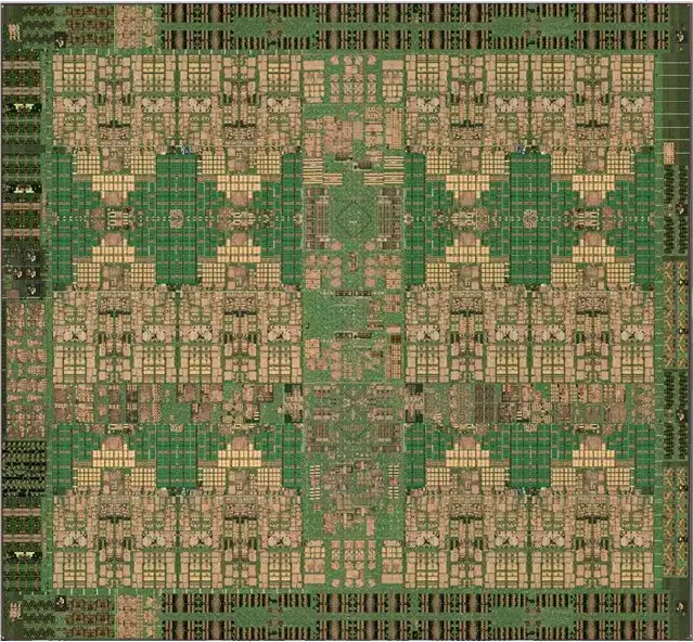
Unlike most of our previous reports, GlobalFoundries 14HP is already here and shipping IBM’s monster ~700 mm² server microprocessors operating at over 5 GHz, packing 100s of MiB of cache, clearly meeting the targets they aimed for. This is made possible through their transition from a planar SOI process to a FinFET SOI – the industry first and only such process – and through their highly dense DT structures. The final process is a result of expertise from both IBM and GF through the combination of IBM’s original FinFET SOI devices and GlobalFoundries bulk MOL and BEOL.
One aspect of 14HP we did not discuss is IBM’s monumental paradigm shift as they move from being an integrated device manufacturer (IDM) to designing products in a fabless environment. That’s a whole topic of its own but does lead us to the big question. Is this the end of the road for their FinFET SOI? There are solid advantages to this process which IBM capitalized on to give them an edge over their competitors. Would be interesting to see if GF produces a future shrink or a derivative of this for their foundry customers.
The really big question for us is the fate of IBM’s eDRAM. IBM’s eDRAM technology is a force to be reckoned with and they certainly know it. They exploit this to their advantage by packing a whopping 6 MiB of private L2 as well as a shared 128 MiB of L3 cache on their z14 microprocessor and another 672 MiB of L4 in their control chip!
It’s unclear if IBM’s eDRAM related patents were handed over to GF as part of their deal when they were handed the fabs. And, if this is indeed the case, it would be interesting to see if the technology remains exclusive to IBM or if other foundry customers can access it. If someone like AMD has access to this technology, it could be highly advantageous for them to make use of eDRAM to pack a large amount of additional cache in order to more effectively compete with Intel’s Xeons in the server market through a distinctly unique differentiator.
–
Spotted an error? Help us fix it! Simply select the problematic text and press Ctrl+Enter to notify us.
–