
GlobalFoundries 14HP process, a marriage of two technologies
Back-end
GlobalFoundries 14HP features a whopping 17-layer metal stack, only matched by GlobalFoundries own 7nm process high-performance stack we detailed last year.
| 14HP Stack | ||
|---|---|---|
| Layer | Pitch | Note |
| M1 | 64 nm | 1x |
| M2 | 64 nm | 1x |
| M3 | 64 nm | 1x |
| M4 | 80 nm | 1.3x |
| M5 | 80 nm | 1.3x |
| M6 | 128 nm | 2x |
| M7 | 128 nm | 2x |
| M8 | 128 nm | 2x |
| M9 | 128 nm | 2x |
| M10 | 256 nm | 4x |
| M11 | 256 nm | 4x |
| M12 | 360 nm | 5.6x |
| M13 | 360 nm | 5.6x |
| M14 | 360 nm | 5.6x |
| M15 | 360 nm | 5.6x |
| M16 | 2.4 µm | 40x |
| M17 | 2.4 µm | 40x |
For the most part those layers are fairly standard. Devices are hooked up using standard tungsten stud contacts to the source-drain region through titanium silicide. We noted earlier that this process combined IBM’s original SOI front-end with GlobalFoundries middle-of-line and back-end from their standard 14nm bulk process. It’s worth pointing out that there is a great deal of overlap between their 14HP and GlobalFoundries upcoming 7nm process. While the local interconnect layers in 7LP has shrunk to facilitate denser routing and enable proper device shrink, most of the remaining back-end layers are very similarly defined (80nm, 128nm, 256nm, 360nm, and 2.4 micron). To us this suggest a good amount of co-design and overlap took place between the two technologies which might ultimately result in a smoother ramp-up for their 7nm process.
The two very top uniquely large (40x) layers are designed to allow efficient power and global clock distribution across IBM’s large dies. Those layers are the same pitch as their 22nm and will remain the same pitch for GF’s 7nm. Under the 40x layers are four global signal wiring layers.
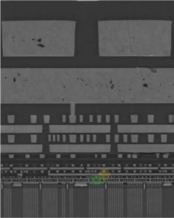
For metal 1 through 3 which has a pitch of 64 nm GlobalFoundries uses double patterning. Unlike Self-Aligned Double Patterning (SADP) used by GF 14nm and 7nm as well as all of Intel’s recent nodes, 14HP uses an alternative patterning technique called litho-etch-litho-etch (LELE) in order to double the pitch density.
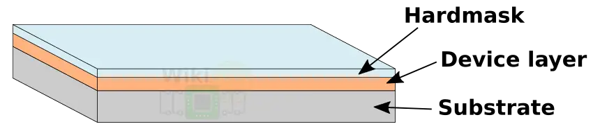
Under LELE you start out with a substrate, the device layer, and the hardmask. The layer is then split into two masks.
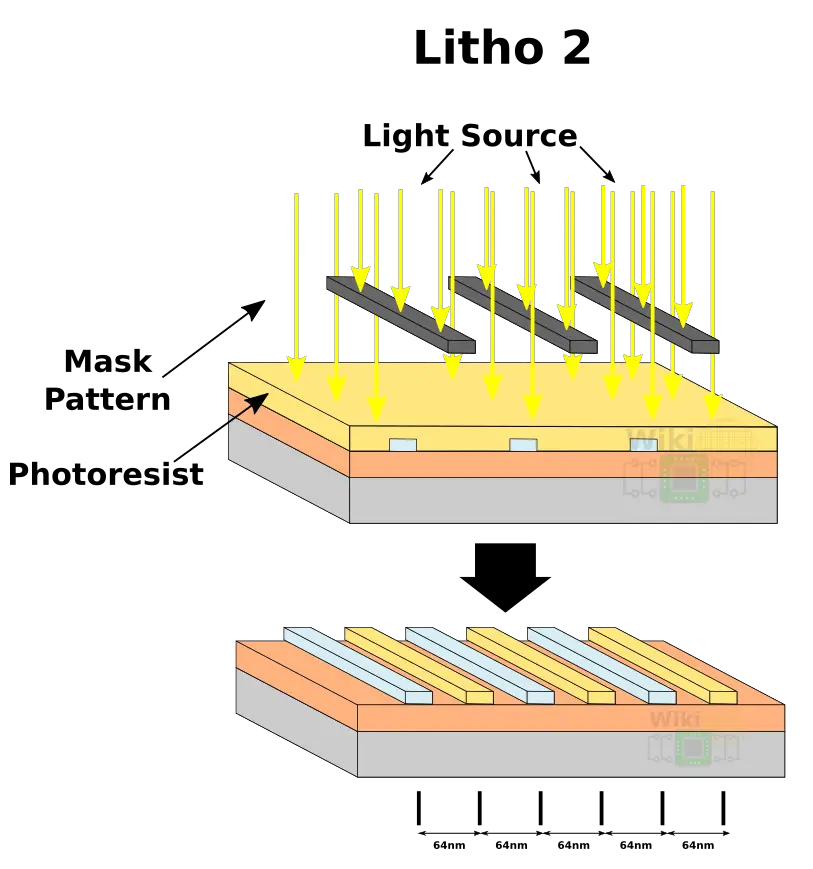
We then apply the photoresist and expose it to light over a mask in order to get the desired pattern. Since our desired minimal metal pitch is 64nm, we can start with a 128nm pattern pitch.
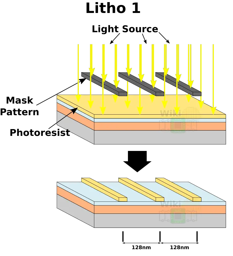
We then transfer the pattern onto the hardmask which will be used for subsequent steps serving as an ad hoc mask.
Now we can shift the pattern and repeat the process with another set of patterns and photoresist using the same 128nm pattern pitch.
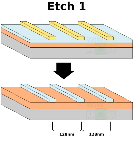
We finally use the hardmask and resist as an etch mask for the underlying device layer.
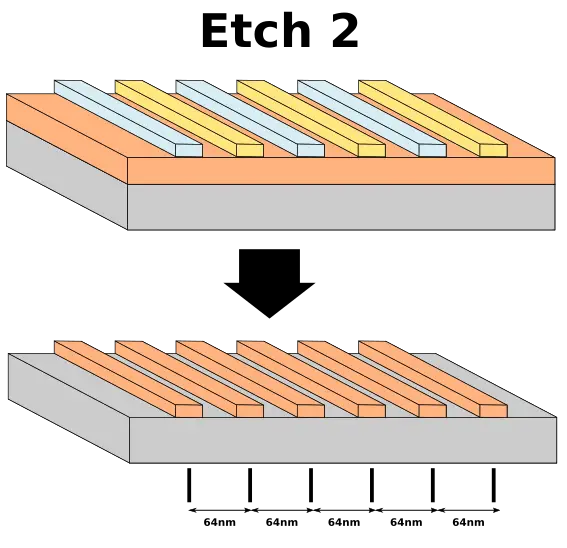
Following the second etch we’re left with the desired pattern where the minimum pitch is achieved is the desired 64nm for this process.
–
Spotted an error? Help us fix it! Simply select the problematic text and press Ctrl+Enter to notify us.
–