
TSMC 7nm HD and HP Cells, 2nd Gen 7nm, And The Snapdragon 855 DTCO
SDM Scaling
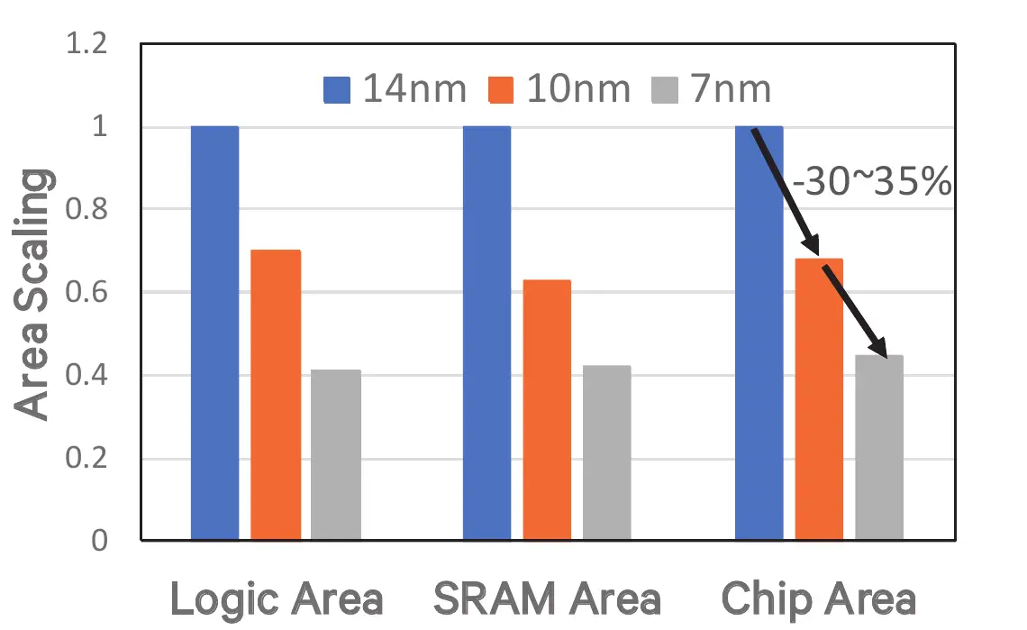
Qualcomm usually reports around a 30% area scaling per generation. With the 7-nanometer node, there it’s no exception. Chi reports that 7 nm enabled Qualcomm to maintain a 30% to 35% area scaling they expect per generation. It’s worth noting that the SDM845 was not fabricated by TSMC but was made at Samsung on their 10-nanometer process. Nonetheless, the scaling is consistent.
Performance
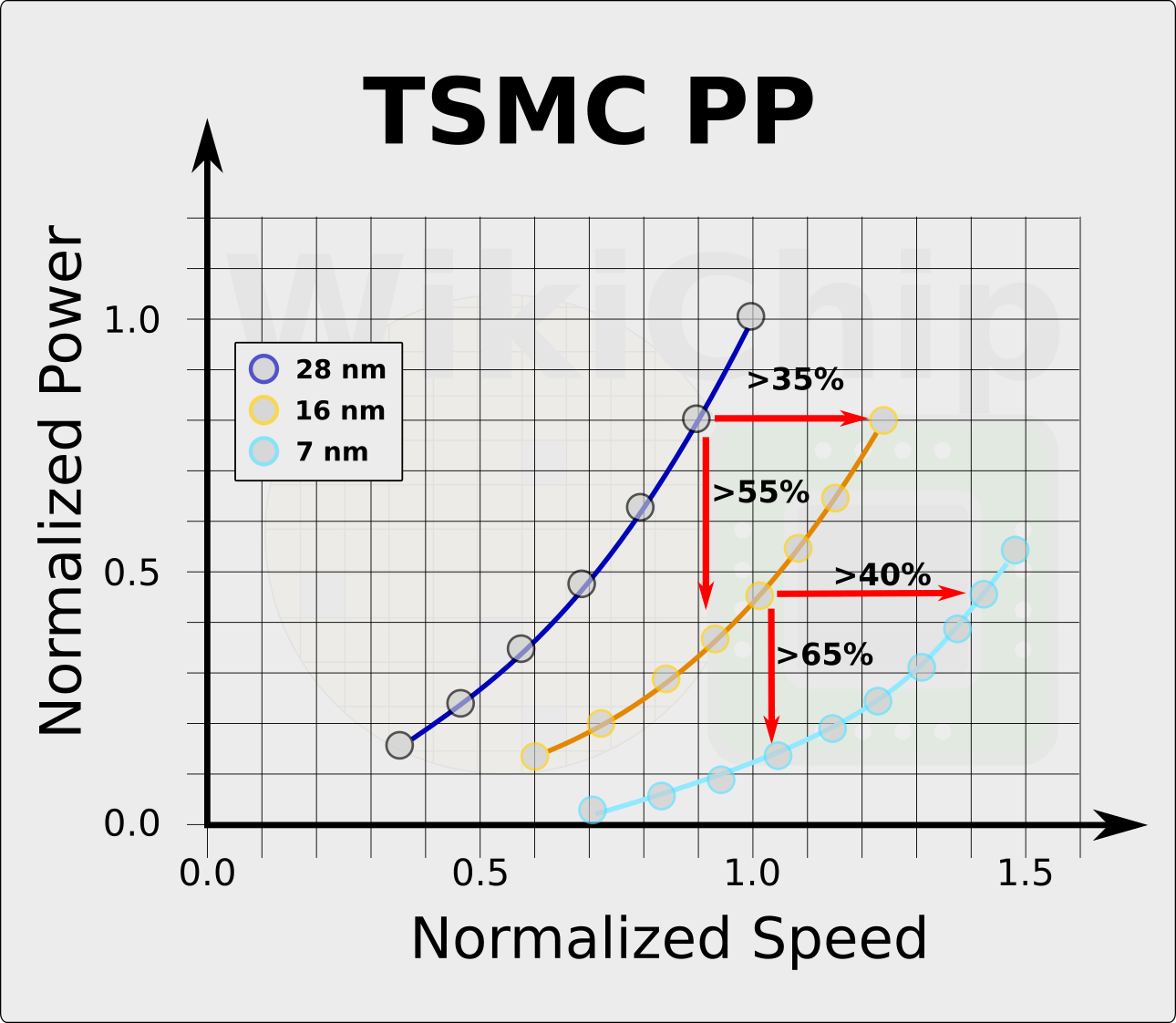
TSMC is reporting up to 40% speed improvement at the same power levels or up to 65% lower power at the same speed.
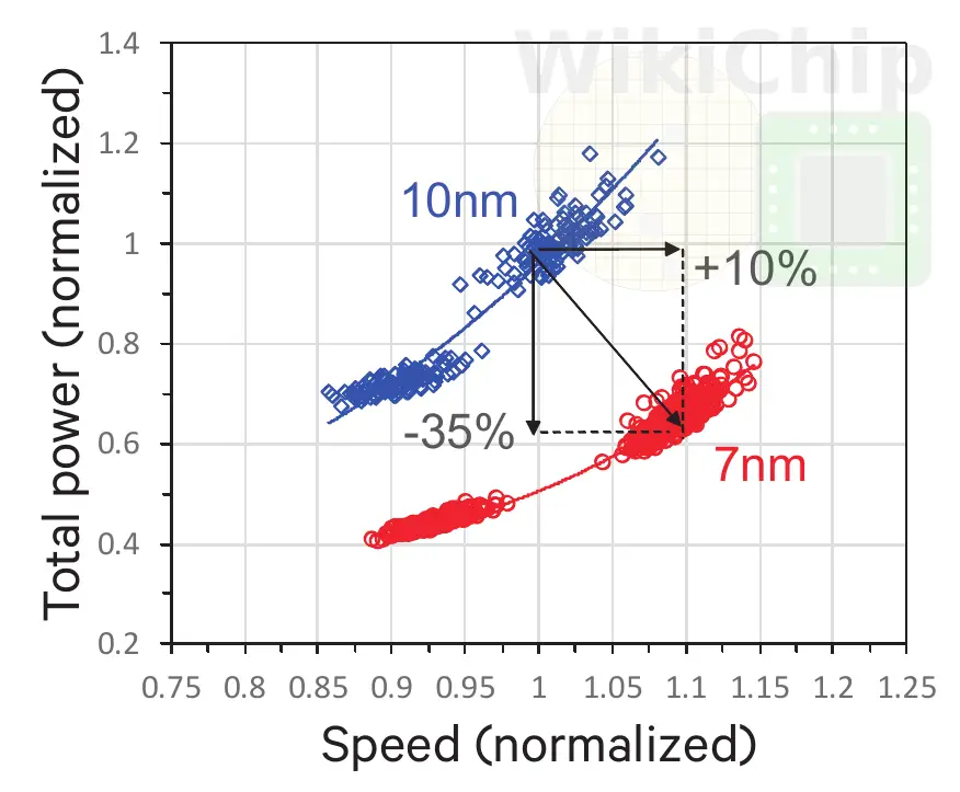
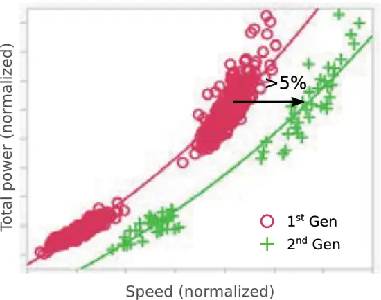
Though those numbers represent best-case numbers from FO4 RO and simple gate measurements, real SoC benefits will be lower. Qualcomm presented a chart comparing the power and speed curves for their critical path design circuits between 10 (Samsung’s) and 7 nanometer. On real critical speed paths on the Snapdragon 855, Qualcomm has reported a 10% speed improvement at identical power and up to 35% lower power at identical speeds. Those are very respectable numbers.
Leveraging Higher Performance Architecturally
For their Snapdragon 855, Qualcomm took full advantage of the new dual-gate pitches offerings. On the Snapdragon 845, Qualcomm used a standard big.LITTLE architecture consisting of four small Cortex-A55 cores along with four big Cortex-A75 cores. The small cores were running at a frequency of 1.7 GHz while the big cores were running at a frequency of 2.8 GHz.
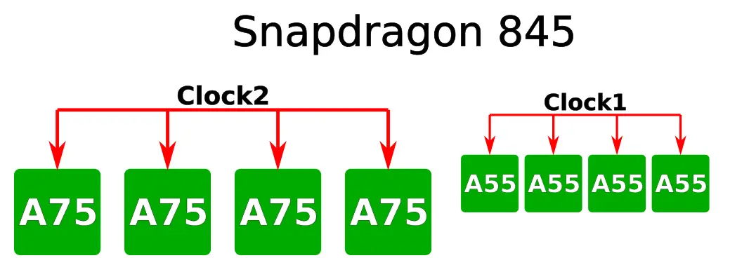
On their latest Snapdragon 855, Qualcomm took advantage of the new HP cells in order to better optimize for performance and power. Here, one of the big cores, called the prime core, were implemented using the high-performance cells while the other three big cores were implemented using the low-power cells. The prime core has a slightly increased frequency of 2.84 GHz while the three remaining cores have a slightly lower frequency of 2.4 GHz. Lastly, the quad-core Cortex-A55 cluster remains largely unchanged albeit with a 100 MHz higher clock. It should be noted that the big cores on the SDM855 have been upgraded to the Arm Cortex-A76, thereby bringing a sizeable IPC improvement which can offset the frequency.
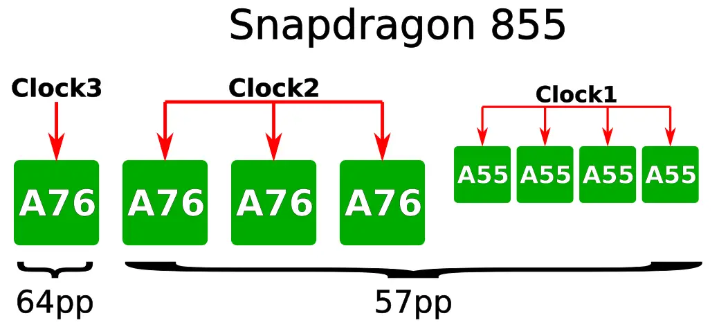
Chi reported that at the same power, Clock2 CPUs have improved by roughly 20% from the SDM845 to the SDM855. With the addition of Clock3, the four cores collectively extend this performance gain over the quad-core cluster on the 845 to over 30%.

From the 845 to the 855 there are two parts that account for the reported “>30% performance”. Those are architectural improvements and process technology improvements. We asked Chi if we could get a breakdown between process and architecture. He told us that more than 50% of the performance can be attributed to architecture improvements. This is a good reminder that having a leading-edge process technology is a necessary but not sufficient condition to delivering a high-performance product.
Dealing With Yield Issues
One interesting aspect of the presentation that Chi delved into was yield. With the original batch of SDM855 processors, they had quite a lot of bad parts rejected by their partners due to high power consumption. A more in-depth look revealed that there was quite a large spread in their Vmin distribution. Naturally, there are two main approaches to handling this specific situation. You can lower the operating voltage or you can tighten the spread distribution. For Vmin higher than the Vdd, the operating voltage has to be raised to pass. Dynamic laser stimulation (DLS) was employed in order to determine the location of sensitive areas. The analysis located flip-flop devices located at a cell boundries. Further analysis revealed physical defects that cause systematic transistor Vt shift, impacting the operating voltage of the critical path. In collaboration with TSMC, design and process changes had to be made to improve the timing margins and reduce the physical defect. Multiple such problems showed up on the 7-nanometer process. A number of key modules that were particularly prone to generating low-voltage defects were isolated including the polycut and RMG clean. Through the DTCO collaboration, the yield loss due to low Vt operations was reduced by 9x. With the help of TSMC, the spread of variation in Vmin was tightened up using device tuning, optimizations across the fin, epi, and the metal gate. All in all, the result is much better uniformity across wafers with power consumption spread being reduced by around 60%. All of this effort is gone into ensuring that the share of parts that are rejected is significantly lowered.
2nd Generation 7nm
TSMC also developed a 2nd generation of their 7nm process. This is an optimized process which uses the same design rules and DUV and is unrelated to 7nm+ which is EUV-based. This process is entirely design-compatible with the first generation but enjoys additional power and performance enhancements. For their second generation process, TSMC made some additional optimizations.
- Fin profile Optimizations
- Epi Optimizations
- MOL resistance Optimizations
- FEOL capacitance
- Metal gate Optimizations
All in all, the 2nd-generation 7nm process is said to deliver over 5% improvement in performance. Additionally, at the same leakage, at high frequencies, the second-generation 7nm process has improved the Vmin by 50 mV. Qualcomm has stated that the second-generation 7-nanometer node will be used for their next-generation cellular 5G modem which will deliver 2x peak data rate over their first-generation 5G modem.
–
Spotted an error? Help us fix it! Simply select the problematic text and press Ctrl+Enter to notify us.
–