
VLSI 2018: Samsung’s 8nm 8LPP, a 10nm extension
Fin Profile, Gate
Samsung reports that the gate length was scaled by roughly five percent (around 1-2nm shorter or so) to get a slight improvement in the gate capacitance.
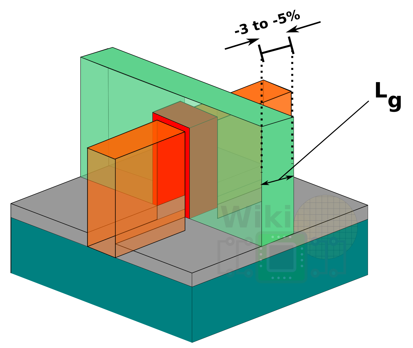
8nm is Samsung’s 5th generation Fin and 4th generation High-κ/metal gate so squeezing whatever little gains are left is getting pretty hard. We do not have a picture to show you, but they made the fins slightly narrower and slightly taller. They are also straighter (note that no actual numbers were given as far as fin dimensions go) to better control the short-channel effects. This was done in order to control the sub-threshold leakage and reduce the parasitic capacitance. They also further refined the replacement metal gate stack in order to increase the drive current. Overall, 8LPP improved the capacitance suppression by a modest 4% over 10LPP.
The reduction in the gate length worsens variations. Their pFETs showed much higher degradation with Lg scaling over their nFETs. To address this, Samsung implemented a couple of process control knobs that optimize the source/drain etch and the embedded silicon-germanium. They claim that the new uniformity knobs have reduced the pFET Vt variations to slightly better than their 10LPP.
Some of the usual optimizations were done in order to reduce the on-resistance. Higher dopant density across the eSD and contact resistance optimizations helped further reduce the Rch and Rext. Compared to their 10LPP process, Samsung reports a contact resistance reduction of 15% for nFET and 9% for pFET. By the way, Samsung calls this “hybrid contact”. What they really mean is that a different cocktail of doping is used for the nFET vs the pFET. They did not delve into any of the details.
Power, Performance
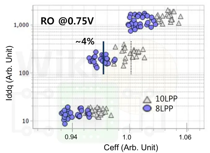
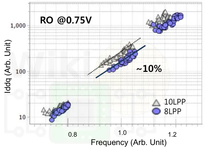
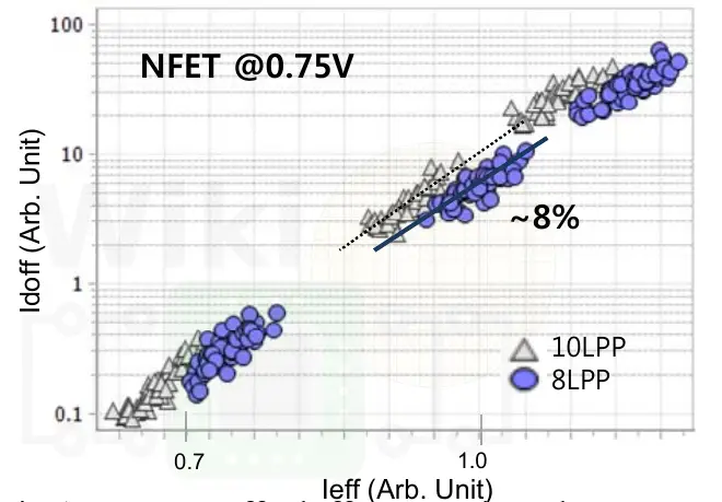
With the various improvements noted earlier, Samsung reported an 8-10% improvement in ring oscillator AC frequency at same IDDQ or conversely, Samsung reports 7-10% power reduction.
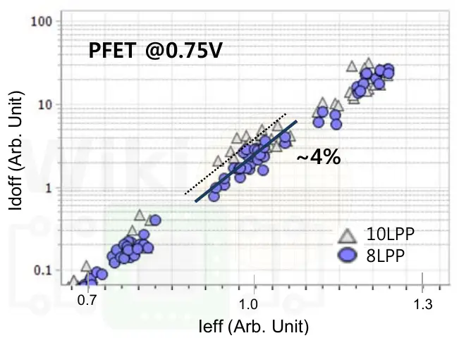
The 8nm pFET contact and eSiGe optimizations produced a performance improvement of around 5% DC gain over 10LPP. Likewise, the nFET S/D and contact optimizations resulted in a 5-8% improvement.
 pFET Performance |
 nFET Performance |
Ultra-low Operating Voltage
One of the other solutions Samsung offers with for 8nm is ultra-low operating voltages for low-power applications such as IoT, AI, and cryptocurrency (yes, they specifically mentioned crypto apps). Those devices exhibit low operation voltage characteristics down to 0.35 V. Samsung reported a 10% improvement in ring oscillator AC frequency at same IDDQ. In an actual CPU product (likely a future Qualcomm chip), Samsung reported 10% power gain over 10LPP for identical Vmin values. For those ultra-low power applications, devices can go down to a single fin which produces larger Idsat variations. To address this, they developed an accurate single-fin model that cover those behaviors.
Yield
Samsung reports D0 yield at similar levels as their 10LPP and says that they can achieve further improvement with design optimizations. Qualcomm is already designing chips for this process and in their own presentation, they also reported that the 8LPP uHD cell has achieved similar yield to the 10nm HD cells.

More Than Stopgap?
A good amount of resources were spent on extracting higher performance and lower power out of their 10nm devices. The metallization stack was changed. The gate was modified. Further effort was spent on introducing a new ultra-high-density cell to go along with this new node. Compared to the changes that were made in 11LPP, 8LPP introduced far more incompatibilities (although all 10LPP IPs can still be used on the 8LPP node). But why? Samsung claims the 8nm is a simple stopgap for their 7nm process. But for a simple stopgap process, Samsung (and Qualcomm) have surely spent a considerable amount of resources – even introducing the industry’s first LE4 quadruple patterning process for the BEOL exclusively for this new node – a process they were very careful to avoid in their 10nm by sticking to the 48nm pitch (to stay within LE3). The level of optimism surrounding the Samsung’s 7nm EUV process at the VLSI symposium was low. The 8nm introductory timing is also suspicious. The consensus at the conference was that the 8nm node is far more than just a stopgap. Most view it as a contingency plan that’s going into effect in order to deliver a marginal advantage while they work to get 7nm off the ground.
–
Spotted an error? Help us fix it! Simply select the problematic text and press Ctrl+Enter to notify us.
–