IBM Chooses Samsung 7nm EUV for Next-Gen POWER and Z Microprocessors
When GlobalFoundries announced they were halting all 7-nanometer process development, there was a lot of uncertainty as to the future of both AMD and IBM. AMD has since announced that Zen 2 will be manufactured on TSMC leading-edge 7 nm process. This left us speculating about IBM. Sources tell WikiChip IBM was considering all three foundries – TSMC, Samsung, and even Intel.
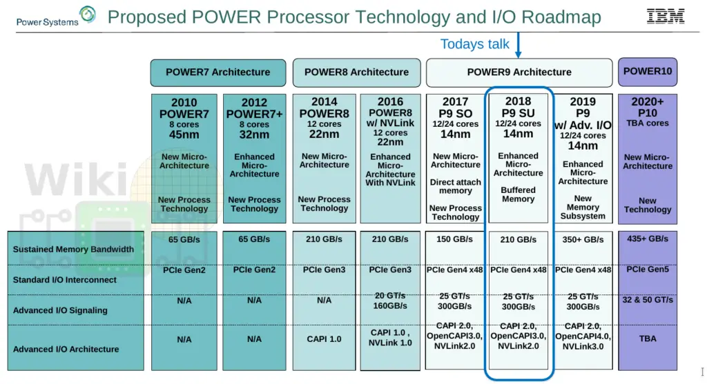
Today, IBM is announcing that they have partnered up with Samsung Foundry for their next-generation of high-performance POWER and Z microprocessors. We recently covered the POWER9 Scale-Up design from Hot Chips. IBM plans one more variant of their 14 nm POWER9 with advanced I/O connectivity for next year.

Power10 is slated for the 2020/21 timeframe. Those will be fabbed by Samsung on their 7-nanometer EUV process. You can find our outline their roadmap here. The company expects 7-nanometer to ramp throughout 2019. “We are excited to expand our decade-long strategic relationship with IBM with our 7nm EUV process technology,” said Ryan Lee, Vice President of Foundry Marketing at Samsung Electronics. “This collaboration is an important milestone for Samsung’s foundry business as it signifies confidence in Samsung’s cutting-edge high performance EUV process technology.”
Renewing the Common Alliance
The decision is not unexpected. IBM, GlobalFoundries, and Samsung are part of the Common Platform Alliance, an R&D process co-design partnership that goes back a few decades. Today, IBM is announcing that they are expanding and extending the 15-year strategic process technology between the two companies. Last year, the Symposium on VLSI Technology and Circuits in Kyoto, the alliance published a paper on stacked nanosheets which they believe will ideal for the 3-nanometer node. This IEDM, Samsung presented their first paper on their GAA transistor for the 3nm node.
–
Spotted an error? Help us fix it! Simply select the problematic text and press Ctrl+Enter to notify us.
–

