TSMC Announces 2x Reticle CoWoS For Next-Gen 5nm HPC Applications
TSMC continuously improves its Chip-on-Wafer-on-Substrate (CoWoS) technology. Today, the company is announcing that, through a collaboration with Broadcom, it is introducing an enhanced CoWoS packaging technology supporting the full 2x reticle size interposers, the largest announced to date. As part of the collaboration, Broadcom defined the top-die, interposer, and HBM configuration while TSMC developed the packaging manufacturing process. With the current i193 and EUV lithography steppers, you are looking at a maximum reticle field size of 26 mm by 33 mm or 858 mm². The new CoWoS enhancement enables chips up to around 1716 mm² in order to enable the larger HPC applications such as HBM-based CPUs and GPUs. TSMC says that the new CoWoS packaging technology is being ready to support its upcoming 5-nanometer node.
TSMC says the new CoWoS packaging technology can accommodate multiple logic dies as well as up to six high-bandwidth memory stacks. As far as memory goes, up to 96 GiB of HBM memory or 16 GiB a stack is supported with bandwidths of up to 2.7 TB/s which is roughly 2.2x the currently highest memory bandwidth. For example, Intel’s recently axed Spring Crest has a memory bandwidth of 1.23 TB/s while NEC’s SX-Aurora tops out at 1.22 TB/s. Support for larger memory comes from Samsung’s new HBM2E dies which goes under the Flashbolt brand. These dies double the density to 16 gigabits per die and with each supporting up to 3.2 GT/s, this translates to 2.46 TB/s for six stacks.
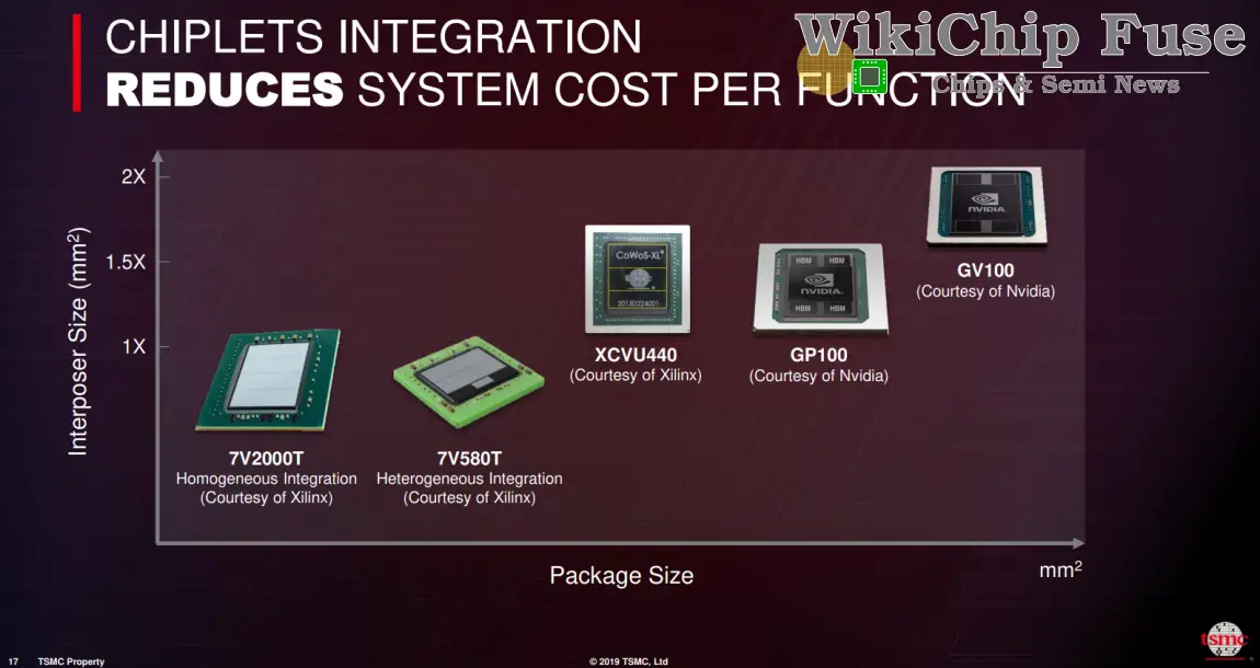
The extension to full 2x reticle is largely a very evolutional announcement. TSMC has been increasing the capabilities of its CoWoS technology for the past half-decade. By 2016 TSMC extended the size of largest CoWoS products to 1.5x. This has enables products such as the Nvidia Pascal P100 to extend to 4 HBM stacks with a 1200 mm² interposer. By 2017 TSMC increased that to 1.75x with products such as NEC SX-Aurora and the V100. Finally, with today’s announcement, TSMC is reaching the 2x reticle size.
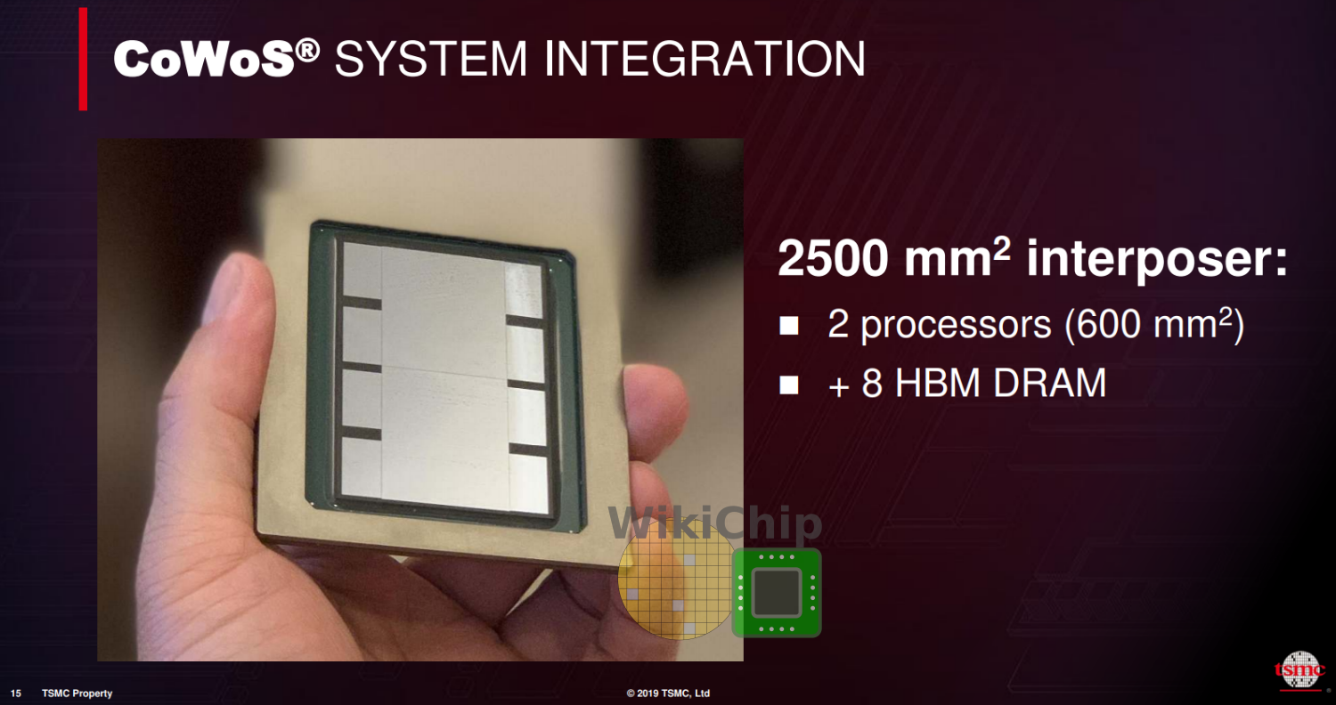
Looking a little further, TSMC has plans for even larger interposers with up to 3x the reticle size or even larger. At three times the reticle, this means interposers of up to 2574 mm². Last year the company showed off a massive 7.5 x 7.5 cm² package with two large 600 mm² dies along with eight stacks of HBM memory. No word on when we can expect the technology to make it to market.
–
Spotted an error? Help us fix it! Simply select the problematic text and press Ctrl+Enter to notify us.
–


