
Nantero’s NRAM, A Universal Memory Candidate?
Scaling
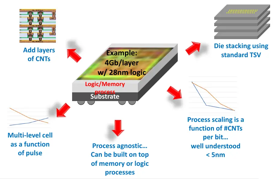
Given all the trouble the industry is going through to scale DRAM, NRAM scaling is an important topic. In fact, we mostly scale DRAM today by simply building more fabs – an unsustainable scaling model. On the other, NRAM shows an abundance of scaling paths. The main issue with scaling DRAM is the capacitor. Scaling the DRAM cell means scaling the capacitors but those capacitors must be capable of storing a minimum amount of storage to reliably maintain the state of a bit. This is proving to be a near-impossible task since the capacitors are already as tall and as thin as mechanically possible from a reliability standpoint. NRAM doesn’t store a charge and should continue to scale to small process nodes. Nantero claims that scaling down to a 5nm node and below is well researched and understood. They went as far as to say that they should be able to go all the way down to a hypothetical 1nm node. With each of those lithography nodes, scaling the NRAM cell involves adjusting the length and the diameter of the CNTs to match the target process, the rest is largely lithography-limited.
Beyond standard lithography, since NRAM is embedded in the BEOL, it’s possible to simply add multiple layers of NRAM across multiple metal layers. In fact, for their first reference product, Nantero designed a DRAM-replacement chip featuring 4 NRAM layers. Alternatively, Nantero is researching multi-level NRAM cells built as a function of the pulse. That one might get them to near flash density. Beyond those methods, standard die stacking techniques are also supported, compatible with DRAM.
A True DRAM Replacement
Nantero is currently working on their first reference product – a drop-in DRAM replacement. And they really mean a drop-in replacement – down to the exact JEDEC specs – performance, timing, power, and unlimited endurance requirements. At Hot Chips they announced that this design is complete. On a standard 28nm CMOS process, Nantero is currently getting 4 Gb per layer in a roughly 100 mm² die. The die itself is a 16 Gb die consisting of 4 NRAM CNT layers which places them at roughly 160 Mb/mm². According to TechInsights, for an 8 Gb die on 1x nm, Micron’s density reported at 137 Mb/mm² and Samsung is at 189 Mb/mm2. From that respect, Nantero is right where the current leading-edge DRAM is but on an older node.
Looking to the future, Nantero is talking about some very aggressive scaling targets. On 14 nm, they are eyeing around 16 Gb per layer for a 64 Gb device with four layers followed by a 128 Gb device with 8 layers. At 7 nm, they are talking about 64 Gb per layer for 256 Gb and 512 Gb devices.

Their DDR4 NRAM replacement device is very similar to normal DRAM. The block diagram below is their DDR4 NRAM reference architecture. The blue blocks are the normal DDR4 functional units whereas the orange blocks are specific to their NRAM architecture. This is where the DDR4 interface is morphed into their NRAM tiled architecture. They did add a few extra functionalities such as remapping logic for post-package repair. One very interesting functionality that should be pointed out is that they actually went ahead and added a SECDED ECC engine to address the possibility of various reliability issues once they start mass production. This isn’t an easy task since you’re trying to fit ECC on every activation while hitting your timing requirements. Gervasi stated that despite adding ECC, they still met all the JEDEC standard requirements.
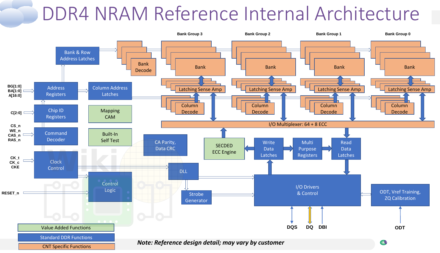
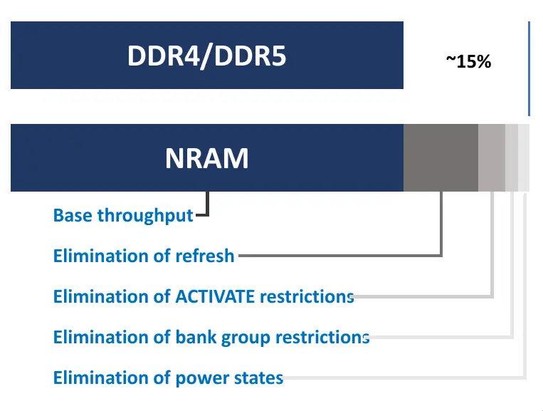
The die is constructed using your standard crosspoint tiles with the decode logic brought into the tile itself with the tile connected to latching sense amplifiers. In your typical DRAM, a requested row is first activated. We then do our read or write after which the row is precharged and is stored back into memory from the buffer. Since the reads and writes are now done on the latching sense amps, the precharge is eliminated and since NRAM is a non-destructive architecture then the refresh is also eliminated. All in all, for identical DDR4 DIMMs, Gervasi says that the NRAM version should have roughly 15% higher effective bandwidth over the DRAM variant.
What’s Next?
Today, Nantero is more or less the commercial spinoff. They license their technology, reference designs, and do various design work for customers (such as the DDR4 replacement device). Currently, Nantero licenses this technology to a number of companies including Fujitsu which says you can expect commercial products next year. While not a universal memory, it certainly comes close – perhaps closer than anything else. NRAM has the potential to disrupt and even replace the DRAM market with seemingly no fatal flaws or gotchas. Whether it remains true and this technology succeeds remains to be seen.
Derived WikiChip articles: Nanotube-RAM.
–
Spotted an error? Help us fix it! Simply select the problematic text and press Ctrl+Enter to notify us.
–