
Intel 2020s Process Technology Roadmap: 10nm+++, 3nm, 2nm, and 1.4nm for 2029
This week IEEE is hosting its flagship process technology conference – IEDM. In a keynote by ASML’s CEO, Martin van den Brink outlined their vision for the future of process technology. Martin highlighted a number of key enabling technologies including the ASML’s own EUV and high-NA EUV machines.
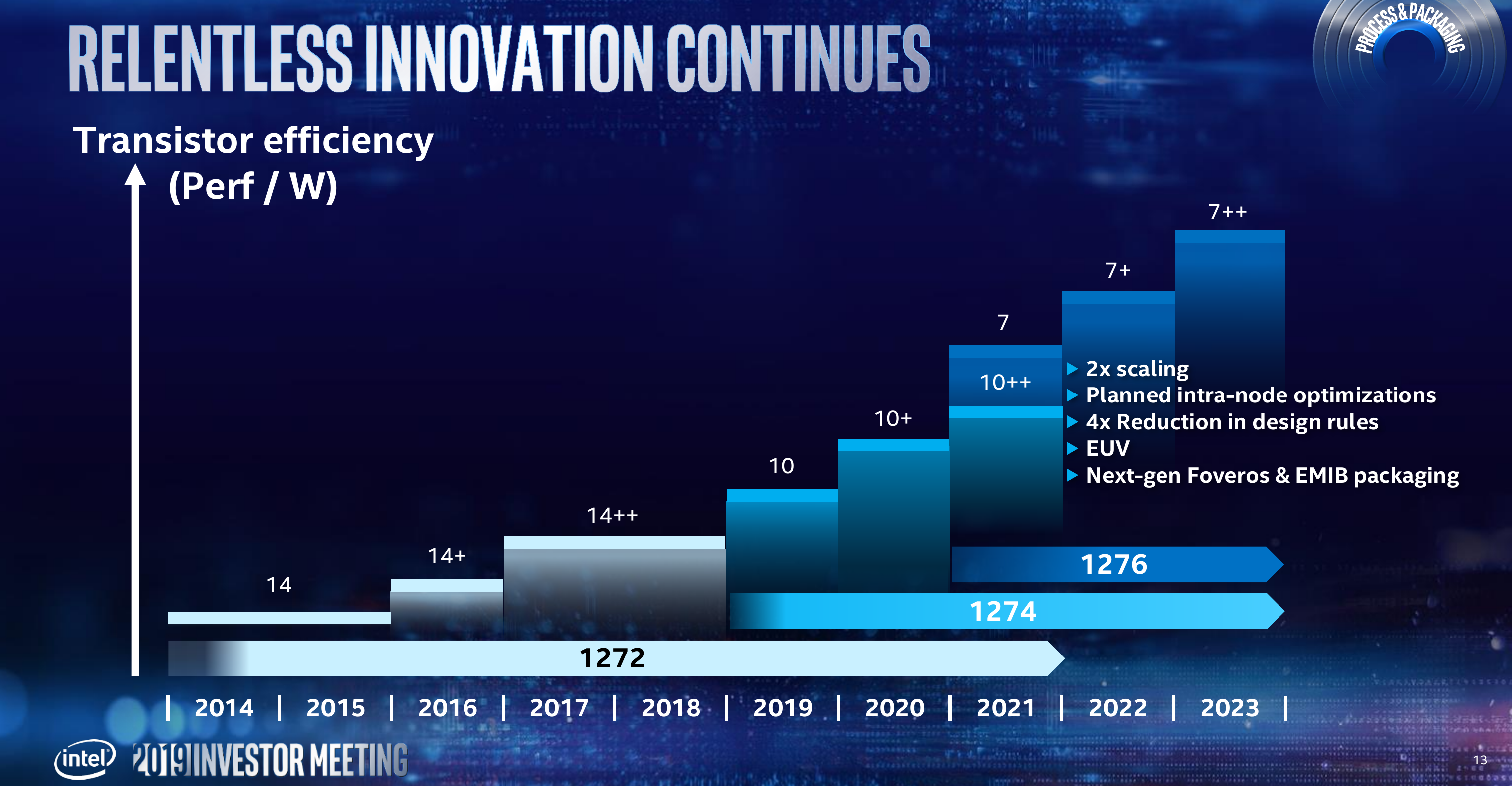
One of the interesting slides Martin presented was about Intel. Intel’s own process technology roadmap got severely derailed when its 10-nanometer process technology encountered major yield issues heading into production. Intel started ramping 10nm only now and heading into 2020, putting them in a difficult situation compared to TSMC. At his keynote, Martin confirmed what Intel re-iterated earlier this year which is that they will be attempting to go back to the usual 2-year cadence. Intel has been fairly vague as far as its 7-nanometer and future nodes are concerned. At his investor meeting presentation, Dr. Murthy Renduchintala, Intel’s chief engineering officer and president of the Technology, Systems Architecture & Client Group confirmed that 7-nanometer will start showing up in 2021, followed by two additional improved nodes going into 2022 and 2023.
Restoring A 2-Year Process Cadence
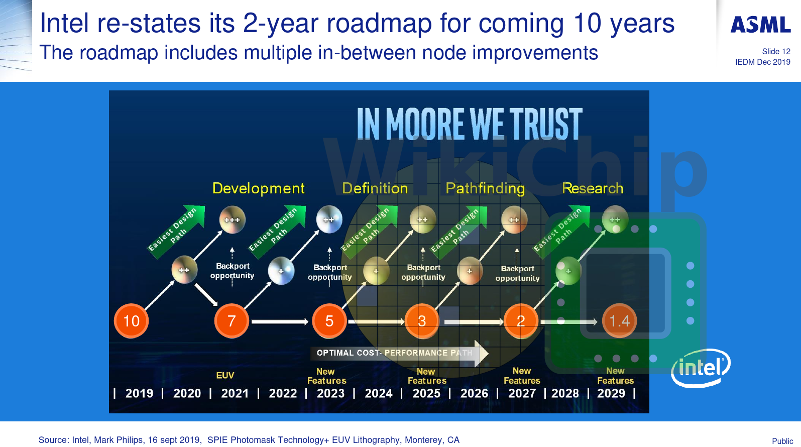
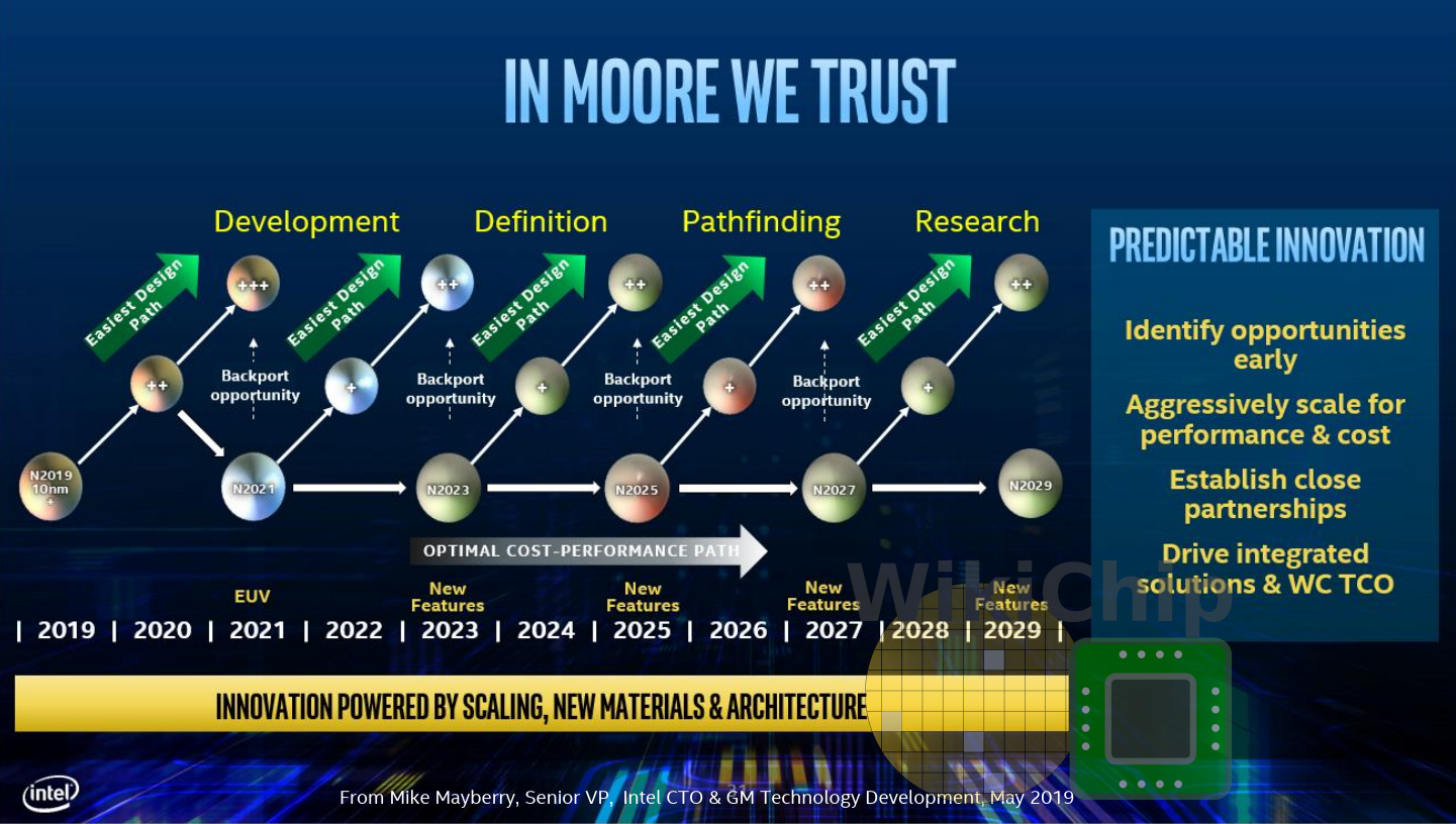
All of that brings up to yesterday’s keynote by Martin. In one of his keynote slides, ASML revealed Intel’s future roadmap – and the slide is literally worth 1000 words.
10nm+++ Shows Up
The first part of the roadmap is particularly interesting. Heading into 2021, you will notice that Intel has a new, unannounced, process “10nm+++” (note the three pluses). This is a further refined version of its 10nm node. Presumably, this will be used for Intel’s Sapphire Rapids CPU which is also planned for 2021. Intel’s 10nm, including 10nm+, has been rather underwhelming as far as the performance goes with only a single SKU exceeding 4 GHz. It would not be unreasonable to expect them to refine the process further in order to enable higher performance chips.
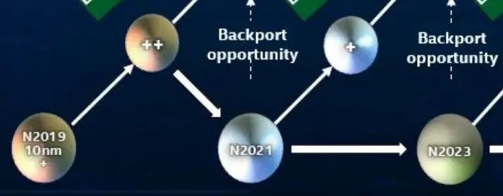
The slide reveals two other more interesting things. The first part is the relationship between the nodes. Notice the arrows for all the ‘base nodes’ come from the prior ‘base node’ with the exception of 7nm. This is expected. But for 7nm, the arrow is actually coming from “10nm++”. We know Intel redefined its 7-nanometer node to address the issues it has had with its 10-nanometer process. This slide goes a step further to implies that 7nm is actually a continuation of “10nm++” and that “10nm+” is more or less orphaned. Intel is also citing backporting opportunities between 7nm and the final 10nm node. Although no details are given beyond just the short note on the slide, at last year’s architecture day, the company talked about being more flexible as far as IP goes, saying that future IPs could be used on more than one node. It looks like this is extended to some of the process features as well.
3nm, 2nm, and 1.4nm for 2029
Heading a little further out, Intel’s 5-nanometer is currently in definition phase while 3 nanometer is pathfinding stage. At last year’s architecture day, Raja Koduri showed that 5 was in pathfinding stages so it looks like things are moving along quickly. 5-nanometer is where we expect Intel to move from FinFET to a gate-all-around (GAA) device. This is also the first “new” roadmap by Intel that concretely goes beyond 3 nm, putting “2 nm” and even “1.4 nm”. Regardless of the node, Intel plans new features at every single node along with the ability to possibly back-port some of those features to the prior more mature node in order to improve it while offering a better design path. It’s also worth pointing out that Intel’s 3-nanometer node coincides with ASML’s high-NA mass production timeline which is around the 2024 timeframe.
Ths roadmap is interesting for a couple of different reasons. First, this is a solid roadmap that shows Intel is, in fact, serious about restoring its two-year cadence. Secondly, although timelines can shift and visibility decreases as we go into node N+3, 1.4nm in 2029 is a long time form now but what’s clear is that the roadmap has been modified to account for the potential of more risks along the way with “+” and “++” subnodes inserted at every node along with the opportunity to back-port features from a future node at each major node transition.
All in all, WikiChip is happy to see Intel remains committed to furthering Moore’s Law for the foreseeable future with an ambitious roadmap. It remains to be seen whether Intel can execute on this roadmap.

Update
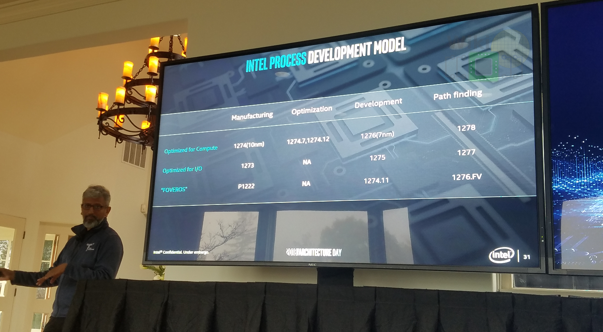
Intel has reached out to WikiChip for a clarification. ASML slide was supposedly taken from Mark Phillips Plenary Session at the International Conference on Extreme Ultraviolet Lithography (EUV) 2019. Further checking revealed that ASML might have altered Intel’s own slide. In particular, ASML edited the slide by changing the bottom dates to actual node names. Regardless of ASML edits to the slide, our analysis remains valid. Furthermore, the guesses for the node names seem reasonable. The original Intel slide is shown below.
–
Spotted an error? Help us fix it! Simply select the problematic text and press Ctrl+Enter to notify us.
–