
ISSCC 2018: MIT’s low-power hardware crypto RISC-V IoT processor
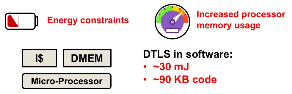
The Internet of Things (IoT) is a rapidly growing and evolving area whereby manufacturers are adding Internet connectivity to every device they make. The ability to connect any device to the Internet brings with it the potential for new and exciting applications. Unfortunately, over the past couple of years, IoT devices have been plagued with security issues. This is partially due to security being implemented as an afterthought, too often, only after the device is breached. But there are more practical reasons why this is such a challenging concept. IoT edge devices operate at very low power, often designed to last years on battery or just on solar power. The protocol of choice for IoT is the Datagram Transport Layer Security (DTLS). DTLS is an IETF-standardized light-weight protocol that provides TLS-based security for UDP-based communication which has been tried and tested for many years. Traditionally, this protocol is implemented by software. However, software implementations are too memory and energy intensive for IoT devices.
![]() This is the challenge a team of MIT researchers have addressed with their low-power IoT processor. At the 65th ISSCC, they presented their paper on their research. The paper was presented by Utsav Banerjee, an MIT graduate student and one of the co-authors of the paper.
This is the challenge a team of MIT researchers have addressed with their low-power IoT processor. At the 65th ISSCC, they presented their paper on their research. The paper was presented by Utsav Banerjee, an MIT graduate student and one of the co-authors of the paper.
The Challenge
The team analyzed existing software implementations on their test platform which pointed to a number of key problems. Their finding revealed that a software-based implementation requires 30 mJ of energy for just the handshake itself. On top of that, the actual code also takes roughly 90 KiB of memory. Thier investigation further revealed that 99% of the DTLS handshake energy is attributed to the elliptic curve cryptography (ECC) operations.
Solution
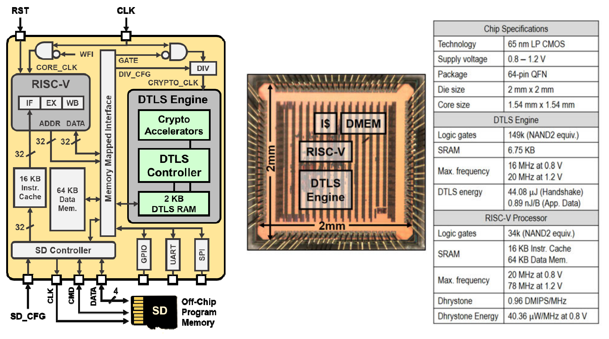
What they came up with is an extension to a typical IoT microprocessor they called the DTLS Engine (DE) which consists of a protocol controller, a dedicated 2 KiB DTLS RAM, and the crypto accelerators.
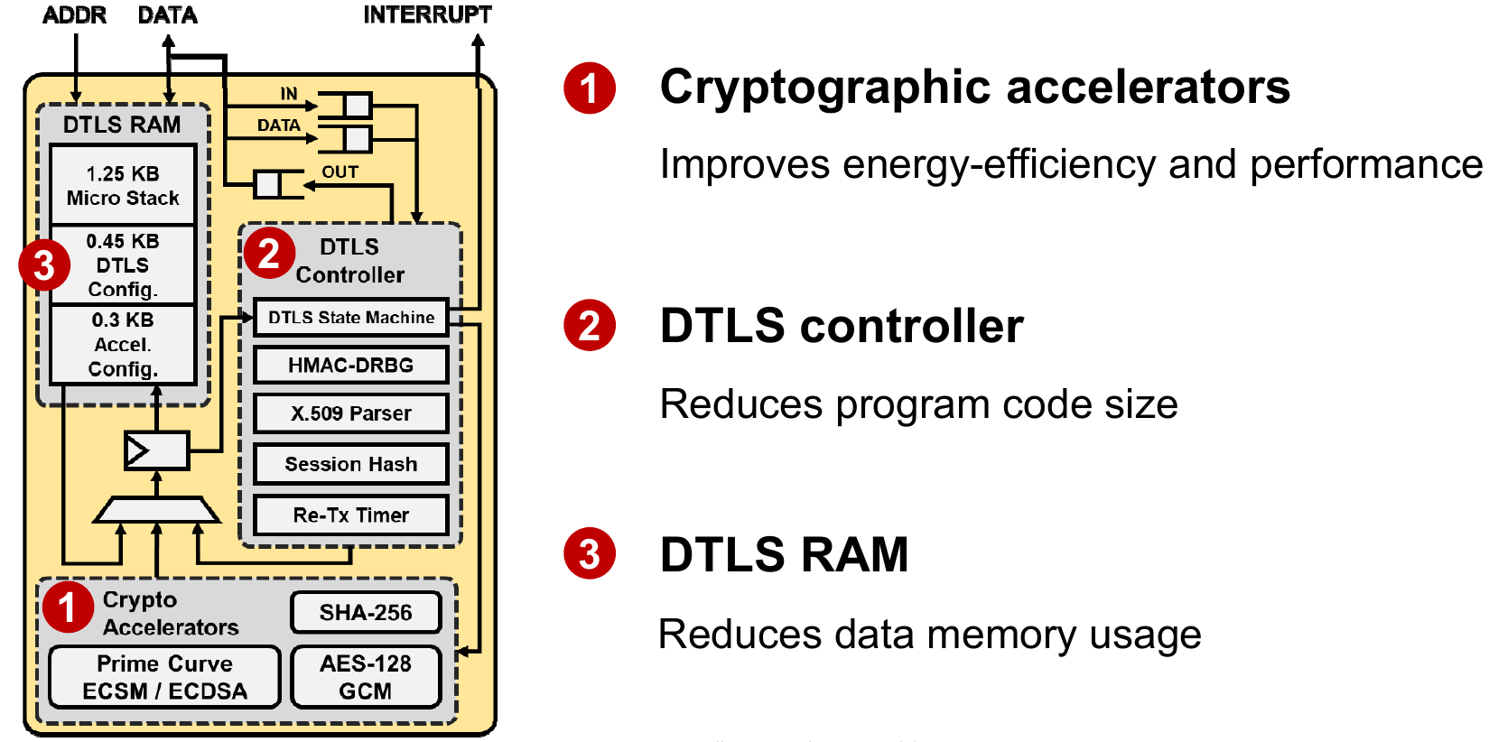
In addition to the AES-128 GCM and SHA-256 accelerators, the DE incorporates a sophisticated prime curve elliptic curve cryptography (ECC) primitives accelerator. When it comes to DTLS, there many different curves and sometimes new curves get recommended to replace older curves which have different security properties. Those curves can be used over different primes with different sizes. To address those possibilities, their implementation was designed to be highly configurable for all existing curves and is compatible with all future-recommended curves.
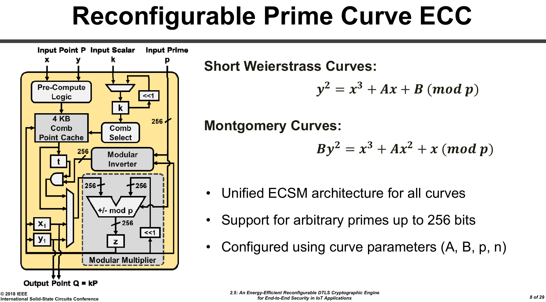
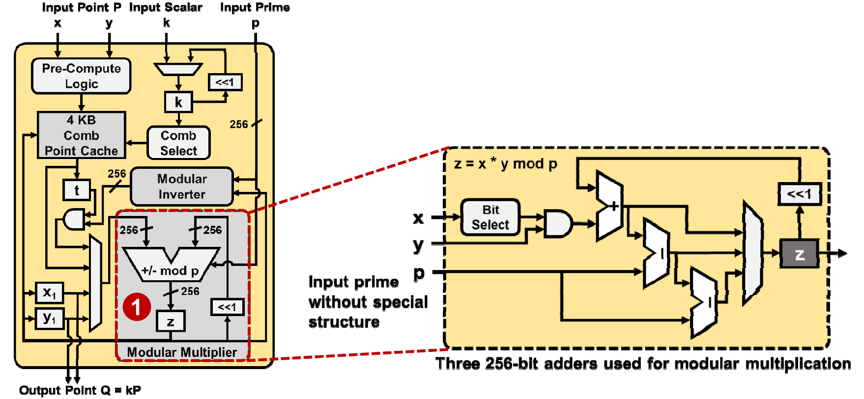
At the heart of the implementation is a modular multiplier which performs interleaved modular reduction. Three 256-bit adders are utilized – one for addition and two for reduction. The algorithm also requires a conditional subtraction which is performed in one cycle. The entire multiplication operation is always performed in constant time in order to prevent timing side channel analysis. It’s worth pointing out that generally, this kind of algorithm would be implemented using 16- or 32-bit arithmetic operations. The choice to handle full 256-bit numbers meant they could eliminate the extra circuitry needed to handle the various smaller operations which resulted in additional energy saving.
The full chip incorporates MIT’s 3-stage RISC-V processor, 16 KiB instruction cache, 64 KiB data memory, an SD card used for storing large programs, the DTLS Engine, and the memory mapped interface used to allow the RISC-V processor to access the DTLS Engine and peripherals. Since some ECC operations can take up to hundreds of thousands of cycles, the processor implements a deep sleep mode which entirely clock gates it when cryptographic operations are taking place. The DE, in turn, uses a dedicated hardware interrupt to wake up the processor upon completion. Additionally, the DE is also capable of caching the server certificate information, speeding up future handshakes.
The chip was fabricated on TSMC’s 65nm LP CMOS process, occupying 2.4 mm² active area, and supporting voltages from 0.8 V to 1.2 V.
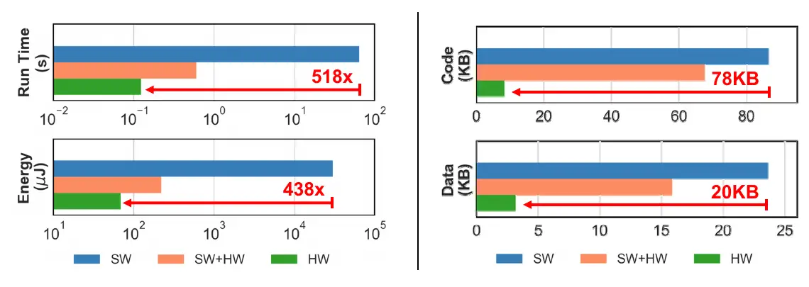
The final result is pretty interesting. Three comparisons were made: full software DTLS on the RISC-V processor (SW), DTLS controller in software and cryptographic primitives in hardware (SW+HW), and full hardware DTLS on the DE (HW).
Compared to the software-only solution, the hardware implementation achieved 518x reduction in execution time and 438x reduction in energy. The energy efficiency is primarily due to the crypto accelerators.
In addition to the energy efficiency, the hardware solution reduced the code size requirements by 78 KiB and data sizes by 20 KiB. The memory reduction is primarily due to the hardware DTLS controller.
The MIT chip has demonstrated that by sacrificing more logic area for implementing a DTLS engine in hardware, a significant reduction in energy and memory requirements can be achieved. The solution not only simplifies software development, but it enables a straightforward and bottom-up approach for developing securely connected IoT devices.
–
Spotted an error? Help us fix it! Simply select the problematic text and press Ctrl+Enter to notify us.
–