VLSI 2018: Samsung’s 8nm 8LPP, a 10nm extension
 Samsung’s 10nm (10LPP) node has been in mass production for over a year now. At the 2018 Symposia on VLSI Technology and Circuits that was held last week, Samsung further disclosed more details about their 2nd generation 10nm node as well as the 8nm extension. 8LPP was presented by Hwasung Rhee, Principal Engineer at Samsung Electronics.
Design Features
As with all leading-edge foundries, Samsung’s 10nm and 8nm technologies are built on many of their existing technologies.
- 4th generation Fins
- 3rd generation High-κ metal gate
- 4th generation S/D engineering
- 2nd generation hybrid N/P
For their 8nm (8LPP) node, just tick +1 all the 10nm generations listed above.
Non-EUV
A key attribute of Samsung’s 8nm node is that it is entirely non-EUV-based. In fact, this is Samsung’s last DUV-base process technology. Going forward, everything will use EUV for the critical layers. Rhee noted “Samsung strongly believe that EUV is the right choice for 7nm. But when we looked at the roadmap, we also observed that there is an empty space between the 10nm and 7nm.” The goal of 8LPP, he explained, was to further push the 10nm node to reach something in the middle. In fact, we believe Samsung is introducing the 8nm node as a Plan B in case they get into trouble with their 7nm node; but more on that later.
Key Dimensions
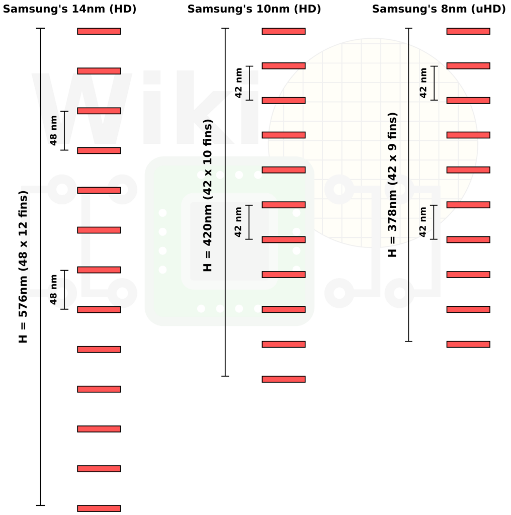
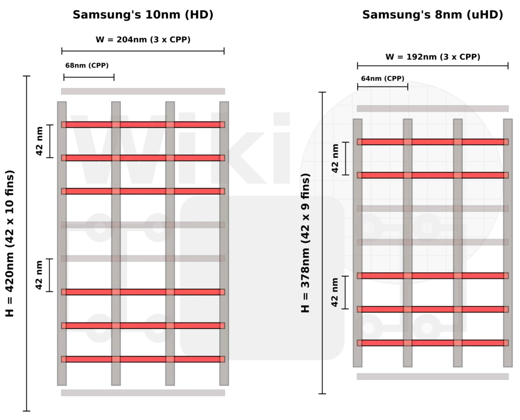
In their VLSI papers, Samsung reports having a poly pitch of 64nm for their 10nm process, but we have confirmed, through Qualcomm, that they actually use a pitch of 68nm. The remaining features are shown below.
| Samsung 10nm | ||
|---|---|---|
| 10 nm | Δ 14nm | |
| Fin Pitch | 42 nm | 0.88x |
| Gate Pitch | 68 nm | 0.87x |
| M1, Mx | 48 nm | 0.75x |
For their 8nm 8LPP, Samsung actually shrunk the gate pitch to 64nm (effectively the original pitch they kept presenting for their 10nm). They also scaled the Mx pitch to 44nm which means they had to resort to quad patterning. Note that Samsung doesn’t use SAQP, but Litho-Etch, Litho-Etch, Litho-Etch, Litho-Etch (LELELELE or LE4), an industry first. Samsung uses LE4 over other techniques such as SADP/SAQP because it gives them greater design flexibility (e.g., bidirectionality) but it does come at an added complexity and issues (e.g., TDDB).
| Samsung 8nm | ||
|---|---|---|
| 8 nm | Δ 10nm | |
| Fin Pitch | 42 nm | 1.00x |
| Gate Pitch | 64 nm | 0.94x |
| M1, Mx | 44 nm | 0.92x |
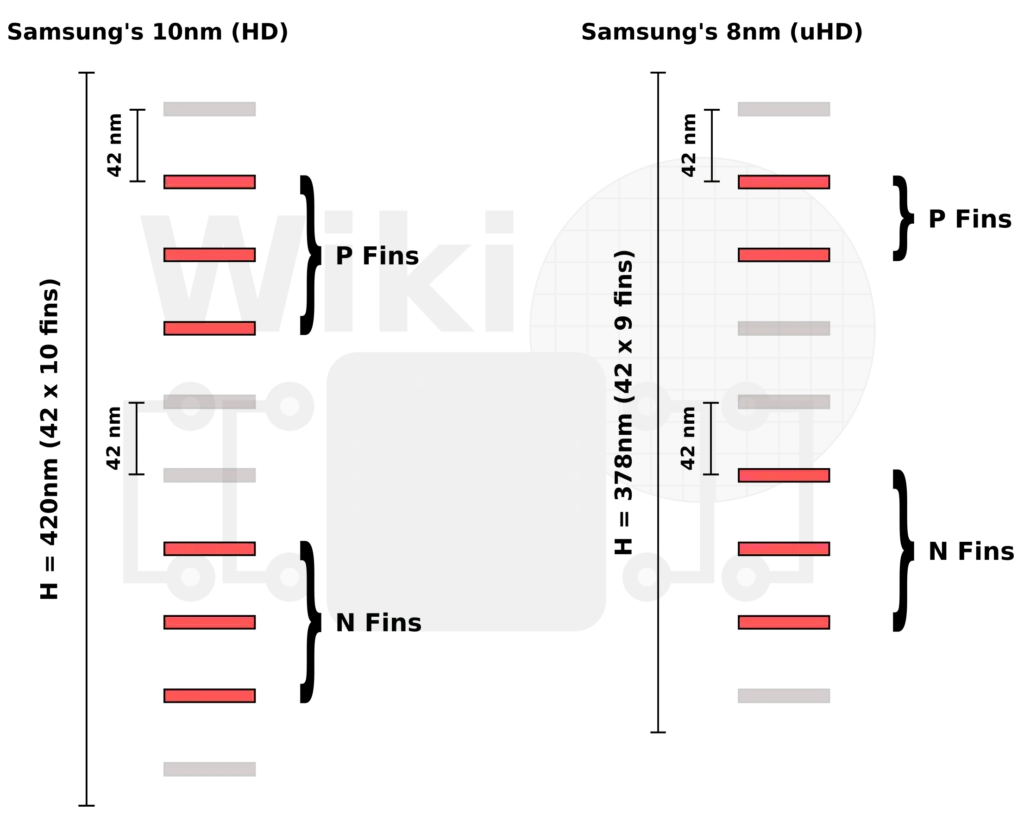
For their 8nm node, Samsung offers two standard cells – high-density (HD) and ultra-high-density (UHD). The high-density cell is identical to the HD cell offered for 10LPP which will enjoy the various power and performance optimizations that were done without large modifications. The UHD cell is a brand new standard cell for 8LPP. This new cell is a single diffusion line pitch lower than the 10nm HD cell (or 0.9x reduction in height) which Samsung claims provides roughly 15% logic area scaling compared with the previous 10LPP cell.

To get that height reduction, 1 P fin has been deducted.

Looking at a NAND2 cell, the area reduction is fairly substantial – around 15% logic density scaling.

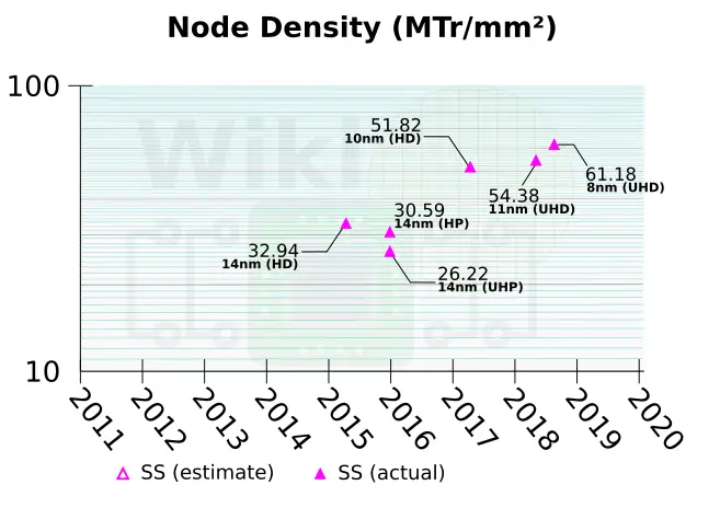
Note that just like their 10nm node, 8LPP uses a single diffusion break. They also added local layout effect (LLE) aware diffusion breaks in order to better address variations. Using the MTr/mm² metric, the new 8nm uHD cell has a transistor density of 61.2 MTr/mm² – Samsung’s highest density non-EUV cell.

–
Spotted an error? Help us fix it! Simply select the problematic text and press Ctrl+Enter to notify us.
–
