AMD Discloses Initial Zen 2 Details
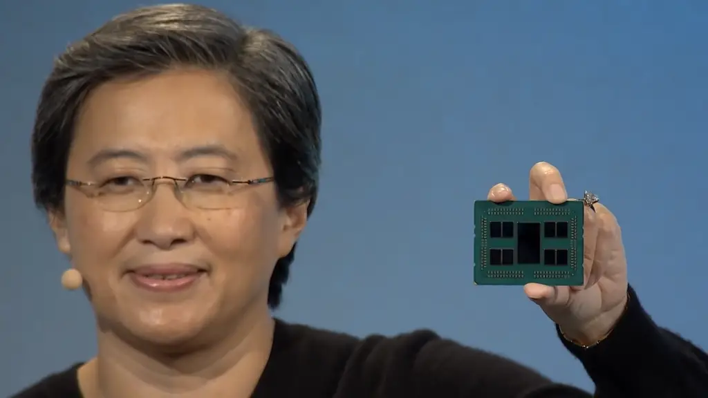
Earlier this month AMD made their first disclosure of Zen 2, their next-generation core microarchitecture for desktop and server chips. Along with Zen 2, AMD also unveiled initial details of their next-generation server chips, codename Rome.
Zen 2

Zen 2 succeeds Zen/Zen+. The design targets TSMC 7 nm process node. AMD evaluated both 10 nm and 7 nm. The choice to go with 7 nm boiled down to the much lower power and higher density they were able to get. AMD claims 7-nanometers delivers 2x the density and offers 0.5x the power at the same performance or >1.25x the performance at the same power (note that at Computex AMD’s slide said “1.35x”). Zen 2-based chips are currently sampling and are on track to be delivered to market in 2019.
AMD has made a large set of enhancements to Zen 2. To feed the widened execution units which were improved in throughput, the front-end had to be adjusted. For that reason, the branch prediction unit has been reworked. This includes improvements to the prefetcher and various undisclosed optimizations to the instruction cache. The µOP cache was also tweaked including changes to the µOP cache tags and the µOP cache itself which has been enlarged to improve the instruction stream throughput. The size of the cache on Zen was 2,048 entries. The exact details of Zen 2 changes were not disclosed at this time.
The majority of the changes to the back-end involve the floating-point units. The most major change is the widening of the data path which has been doubled in width for the floating-point execution units. This includes the load/store operations as well as the FPUs. In Zen, AVX2 is fully supported through the use of two 128-bit micro-ops per instruction. Likewise, the load and store data paths were 128-bit wide. Every cycle, the FPU is capable of receiving 2 loads from the load/store unit, each up to 128 bits. In Zen 2, the data path is now 256 bits. Additionally, the execution units are now 256-bit wide as well, meaning 256-bit AVX operations no longer need to be cracked into two 128-bit micro-ops per instruction. With 2 256-bit FMAs, Zen 2 is capable of 16 FLOPs/cycle, matching that of Intel’s Skylake client core.
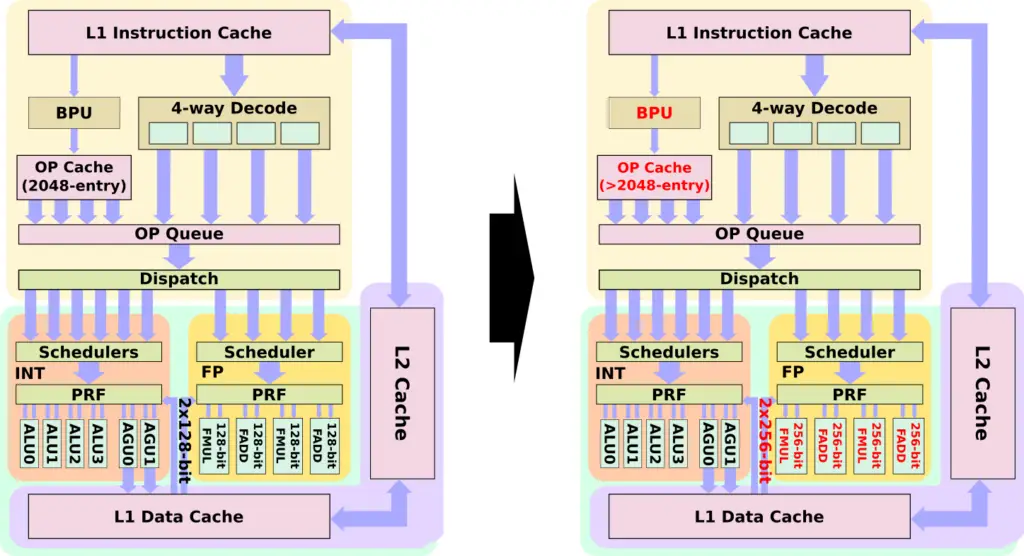
AMD stated that Zen 2 IPC has been improved along with an increase in both the dispatch and retire bandwidth, however, the fine details were not disclosed. On the security side, Zen 2 introduces in-silicon enhanced Spectre mitigations that were originally offered in firmware and software in Zen.
Rome
Some people called it [chiplets] gluing things together; we called it the next generation of system design. – Dr. Lisa Su, AMD President and CEO
AMD’s second-generation EPYC is codename Rome, the successor to Naples. The two are socket and platform compatible. Note that Milan, Rome’s sucessor, is also socket compatible. Rome still uses a multi-chip approach to scale up the core count but the system design itself has changed quite radically from the prior generation. In Naples, AMD scales up the 8-core design, called a Zeppelin, to 32 cores by stiching together four of those SoCs through their proprietary interconnect called the Infinity Fabric. This method provided eight memory channels and 128 PCIe lanes distributed accross all the dies.
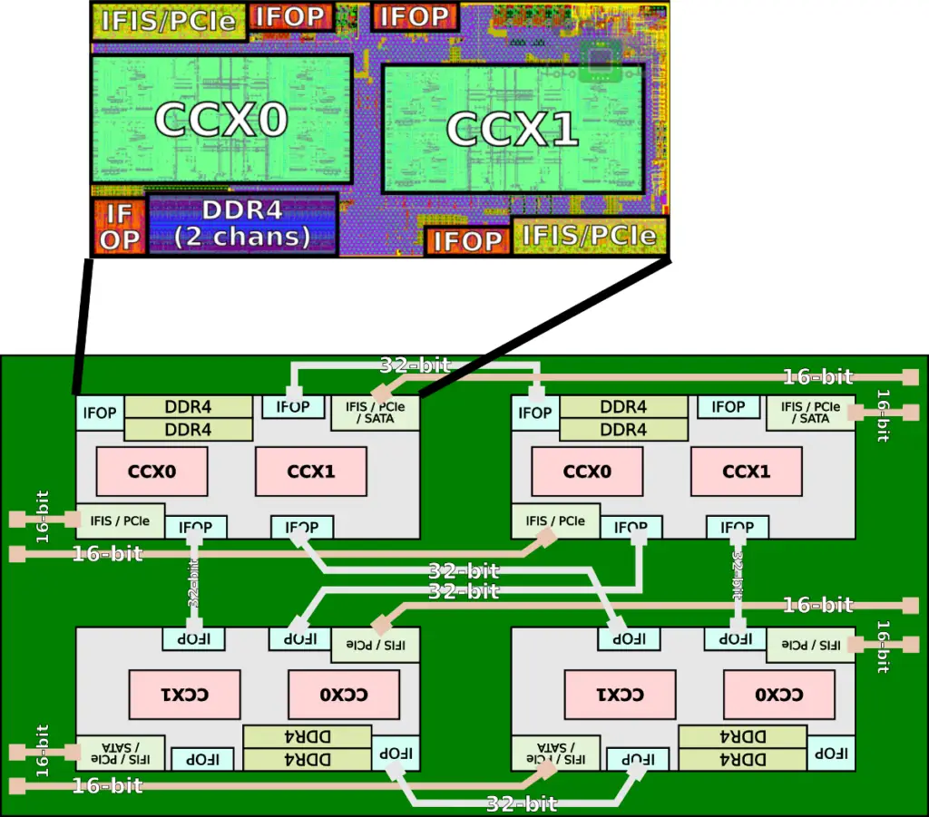
With Rome, AMD is taking the idea of chiplets further. Similar to what they initially started with Threadripper 2, Rome has compute dies and an I/O die. However, this time, AMD took out the core execution blocks and moved them to new compute dies, leveraging TSMC’s 7 nm process and taking advantage of the lower power and higher density. The compute dies are then connected to a centralized I/O die that manages the I/O and the memory. The much bigger I/O die is manufactured on GlobalFoundries mature 14 nm process where most the power and density cannot be realized.
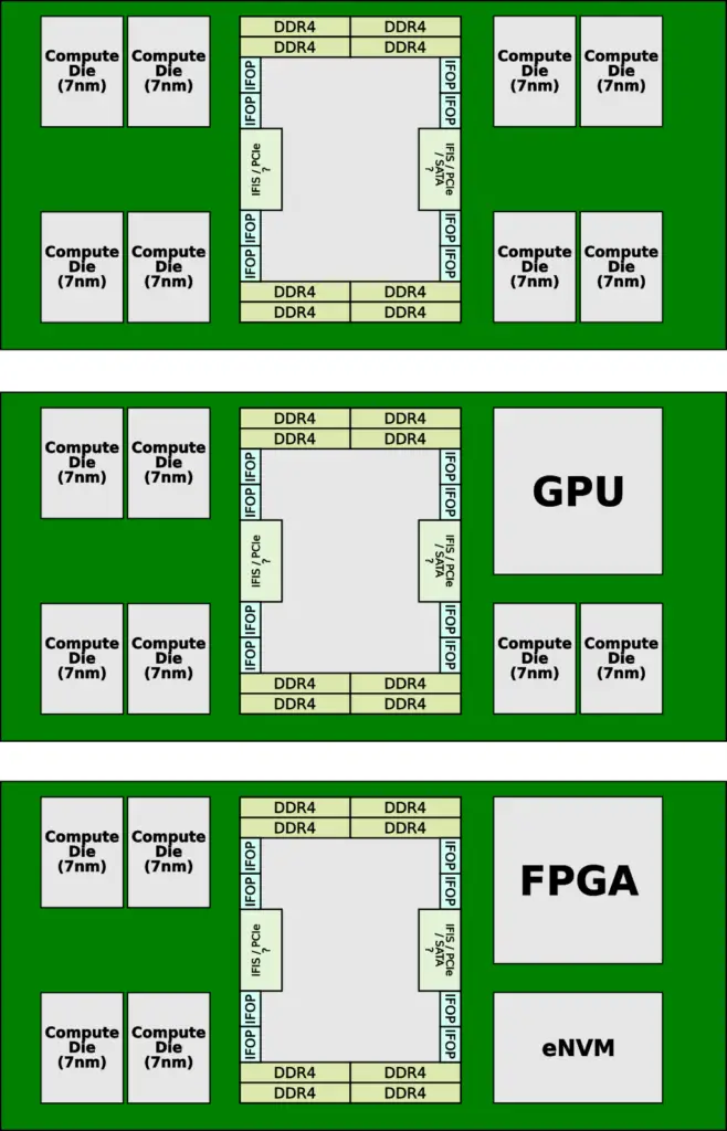
In total, there are nine dies. One I/O die and eight compute dies – each with 8 Zen 2 cores. Neither the details of the individual compute dies nor the I/O die were disclosed. There are a fair bit of challenges involved in this kind of design and it would be interesting to see how they were addressed. The I/O die creates deterministic and unified latencies across the entire chip, but it would potentially affect best-case/sensitive scenarios. The package is organized in four pairs of compute dies similar to our diagram below. It’s worth noting that each pair of compute dies are packaged tightly together on the organic substrate, indicating there might be very short traces going between them.

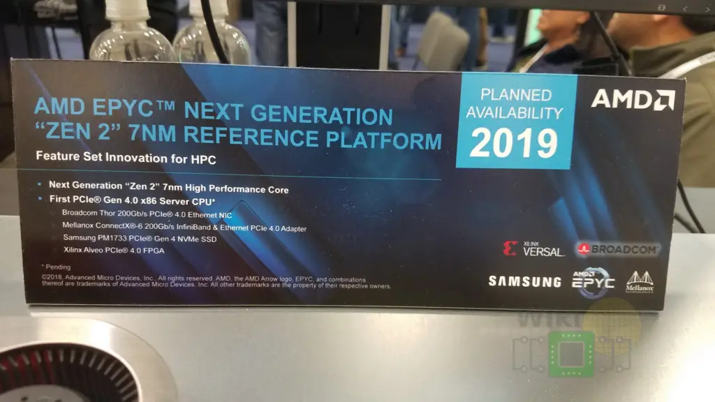
With eight octa-core compute dies, Rome can offer up to 64 cores and 128 threads, effectively doubling/quadrupling (AVX2) the throughput of first-generation EPYC. Although Rome stays with 128 PCIe lanes, it brings new supports for PCIe Gen 4, doubling the transfer rate from 8 GT/s to 16 GT/s. There are eight DDR4 memory channels supporting up to four terabytes of DRAM per socket. One interesting detail AMD disclosed with their GPU announcement is that the infinity fabric now supports 100 GB/s (BiDir) per link. If we assume the Infinity Fabric 2 still uses 16 differential pairs as with first-generation IF, it would mean the IF 2 now operates at 25 GT/s, identical to NVLink 2.0 data rate. However, since AMD’s IF is twice as wide, it provides twice the bandwidth per link over Nvidia’s NVLink.
One of the things EPYC brought is SME and on top of that SVE which extended SME to AMD-V, allowing individual VMs to run SME using their own secure keys. With Rome, AMD says the number of keys (and thus VMs) support has also been increased.
I/O Die
There is a lot of mystery surrounding the capabilities of the I/O die and AMD’s plan for the future. By moving all the “redundant components”, such as the I/O and southbridge, from the compute die to the I/O die, AMD has opened up their design to some intriguing possibilities. Since all the controls can be found in the centralized I/O die, it becomes possible to swap out the compute dies with other types of logic such as an FPGA (e.g., from Xilinx) or a GPU. In Naples, this would have meant sacrificing some of the I/O or memory but with Rome, this is no longer the case. AMD has not announced any such plans, but the option is there.
Roadmap

The key takeaway from AMD’s event is their roadmap. A predictable roadmap helps improve customers confidence in the platform. AMD wanted to show that they are capable of laying out a roadmap and execute on it. To that end, AMD expects Zen 2 to launch in 2019. Zen 3 is on track and Zen 4 is at the design completion phase.
–
Spotted an error? Help us fix it! Simply select the problematic text and press Ctrl+Enter to notify us.
–


