
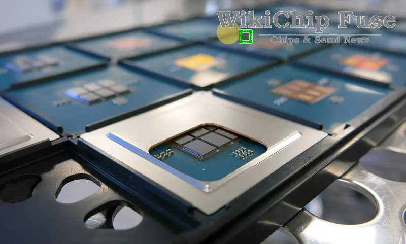
CEA-Leti Demos a 6-Chiplet 96-Core 3D-Stacked MIPS Processor
Beyond traditional scaling, a major trend that has been emerging over the last few years is heterogeneous integration. The industry is looking to extend the functionality of an SoC to a wider range of accelerators beyond traditional compute. At the recent ISSCC 2020 conference, CEA-Leti has taken a stab at the problem with their own project.
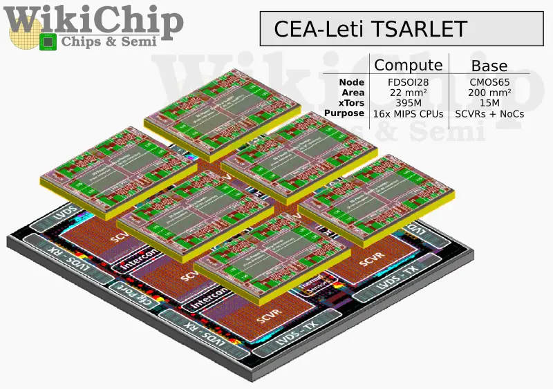
The chip designed is called TSARLET. In order to demonstrate the theoretical capabilities of a highly-modular SoC, researchers from CEA-Leti built up the fairly complex SoC using 6 chiplets that are 3D-stacked on top of an active interposer base die which provides the chiplet-to-chiplet interconnections as well as the external I/O connectivity. Each chiplet integrate 16 MIPS cores along with the caches and the necessary logic to extend communication beyond the chip. The individual chiplets are made on STMicroelectronics 28nm FD-SOI in order to exploit higher density and lower power while the base die is made on a legacy 65 nm process in order to reduce cost. The chiplets are kept to a minimal size of about 22 mm² in order to maximize yield and reduce cost whereas the base die is measured around 200 mm² – large enough to incorporate all six chiplets.
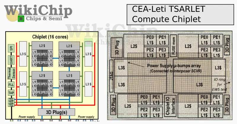
Delving a bit deeper, each chiplet comprises four quad-core clusters. Being a technology demonstration, the cores themselves are fairly simple scalar MIPS32v1 core with a private 16 KiB of L1I$ and L1D$ but the architecture should easily scale to much more complex cores. There is 256 KiB of L2 cache per cluster and four 1 MiB tiles of L3 cache. As you can imagine, the chiplet is most dominated by SRAM. Four levels of interconnects have been implemented. The chiplet implements a NUMA architecture. Within each quad-core cluster inter-core communication is done via a crossbar that links all the L1 (instruction and data) caches together. L1 cache coherency is maintained by the L2 caches using a directory-based protocol with a linked-list directory. Lines are in either list mode where modifying shared data causes a multicast update message to get issued or in counter mode which caps the number of sharers to four on this SoC, invalidating everyone else.
In order to extend the cache coherency and communication throughout the full chip, three additional NoCs are implemented. There is a short-reach 5-channel 2D-mesh interconnect implementing the cache coherency protocol. Between the L2 and L3 there is a 2-channel 2D-mesh long-reach interconnect that is also extended in the 3D direction. Lastly, between the L3 caches there is a similar 2-channel 2D/3D-mesh interconnect which is also extended to the off-chip DRAM memory.
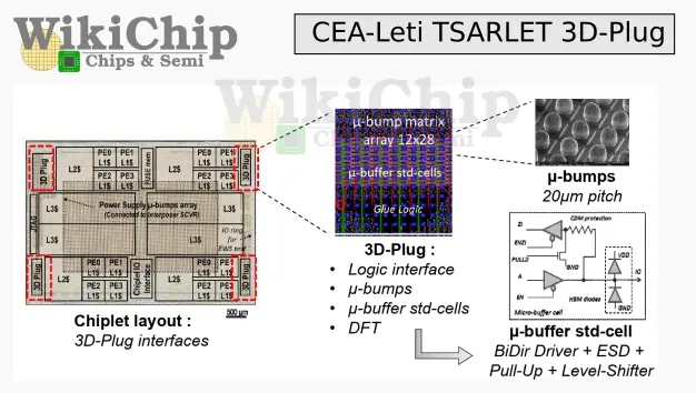
One of the key components the Leti researchers developed for this chip is the custom 3D interface, the 3D-Plug. The 3D-Plug is a generic chiplet-to-interposer interface designed to allow any sort of chiplet to communicate with other chiplets that land on the base interposer die. Two implementations of the 3D-Plug were designed. The first is a source-synchronous version designed for 2.5D passive links designed for short reach and low latency connections. The L1-L2 NoCs utilize this interconnect. The second implementation is the asynchronous version which relies on quasi-delay quasi-delay-insensitive logic using 1-of-4 data encoding without clocking. 4-phase is used for on-die communication within the interposer while using 2-phase for off-die communication at the 3D-plug interface. A 4-phase-to-2-phase protocol conversion was introduced to convert between the two.
Depending on the distance, latency for the passive link (L1-L2) can range from 7.2 ns to 44 ns for the farthest link due to re-timers. For the L2-L3 best end-to-end latency is 15.2 ns. Leti reported quite a lot of data. The interesting numbers are the propagation speeds and power efficiency associated with those links as they give us a pretty nice compared to other multi-chip designs such as AMD’s. For the passive links, they are reporting sub-0.3 pJ/bit/mm. For the active links, they are reporting power efficiency of around 0.52 pJ/bit/mm.
| Interconnects | ||||
|---|---|---|---|---|
| Link | L1-L2 Nearest |
L1-L2 Farthest |
L2-L3 4-Phase |
L2-L3 2-Phase |
| E-to-E Latency | 7.2 ns | 44 ns | 15.2 ns | 15.2 |
| Propagation | 4.8 ns/mm | 2.9 ns/mm | 0.6 ns/mm | 0.6 ns/mm |
| Energy Efficiency | 0.29 pJ/bit/mm | 0.15 pJ/bit/mm | 0.52 pJ/bit/mm | 0.52 pJ/bit/mm |
There are four 3D-Plugs on each chiplet corresponding to the four compute clusters within the die – each one is physically located at the corner of the die. The interfaces comprise a μ-bump matrix array of 12 x 28 μ-bumps with a 20 μm pitch which is one of the most aggressive bumps we have seen reported to date in an SoC demonstration. The high-density interface tops their bandwidth density at 3 Tb/s/mm² while achieving a very good power efficiency of 0.59 pJ/bit.
| 3D-Plug | |
|---|---|
| Bump Pitc | 20 μm |
| Voltage Swing | 1.2 V |
| Data Rate | 1.21 GT/s |
| Power Efficiency | 0.59 pJ/bit |
| Bandwidth Density | 3.0 Tb/s/mm² |
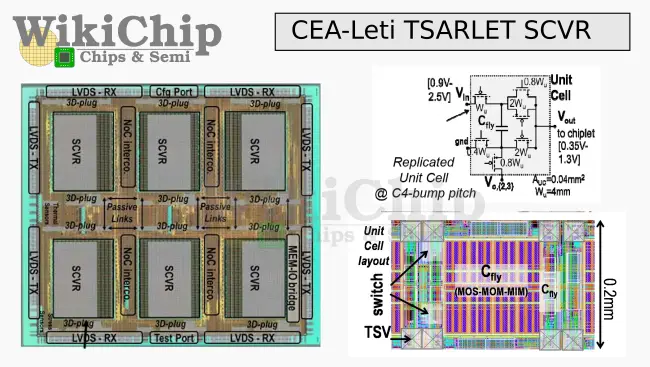
All six chiplets land on the active interposer base die. It provides the interface between the various chiplets using the 3D-Plug interface. In addition to the NoC wiring, the base die integrates six switch cap voltage regulators – one for each chiplet. Each of the SCVRs are managed by a central clock-frequency and feedback controller, allowing rapid transitions and local IR-drop control. The SCVRs are fully integrated using thick oxide transistors with no external passive components. On-chip CAPs are used using MOM+MOM+MIM for a total capacitance density of 8.9 nF/mm².
The relatively high voltage of around 1.8-2.5V is brought to the die from the backside through 40 μm pitch TSV array. This voltage is then stepped down within a 10-phase 3-stage gearbox. For the DVFS mechanism, it supports 7 voltage ratios for a wide range of Vout (0.35V to 1.3V). The SCVRs themselves are designed as a tiled architecture with each SCVR unit consists of 270 instances of the unit cell. Leti reports a power conversion efficiency of 156 mW/mm² at 82% peak efficiency, putting it at better efficiency compared to contemporary integrated LDOs.
Overall, the final chip is capable of operating at 130 MHz at 0.5 V all the way up to 1.15 GHz at 1.1 V. Since the integrated cores are very simple cores, with 2 ops per core, you are looking at a peak compute of 220 gigaOPS. Leti reports at best energy efficiency of 9.6 GOPS/W on Coremark at 246 MHz at 0.6 V. The important power breakdown is the amount wasted on interconnect. Off the total SoC power budget, juts 3% goes the way of interconnects. 17% is spent on all the SCVRs, and 13% is used up by the memory controllers and PHY. The remaining 67% is attributed to the chiplets (11.17% per chiplet). Off the total chiplet power consumption, about 55% is attributed to the cores + L1.
–
Spotted an error? Help us fix it! Simply select the problematic text and press Ctrl+Enter to notify us.
–