
IEDM 2017: AMD’s grand vision for the future of HPC
A Paradigm Shift for the Future of HPC
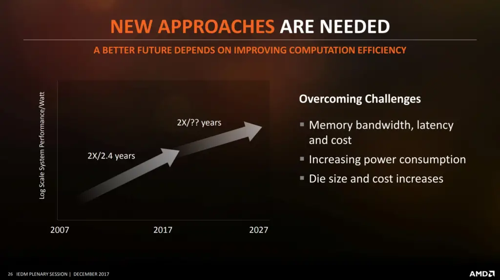
Over the last decade, the performance efficiency has increased at the rate of roughly double every 2.4 years. Su wants to change that. She hopes to actually accelerate the performance efficiency at a higher rate than was previously done.
Breaking Die Constraints
AMD believes that we are at an inflection point for multi-chip architectures. By making smaller chiplets which feature an efficient and scalable die-to-die interconnect fabric, one can use multiple smaller dies to piece together a much larger processor. The idea is certainly not new and various companies have done it before but not in high-volume applications in the area of HPC.
Su used AMD’s own EPYC chips as an example. AMD’s EPYC chips consist of 4 identical chiplets interlinked using AMD’s Infinity Fabric. Each of the chiplets consist of 8 cores and its own set of I/O PHYs. The final product is a very large chip with 32 cores.
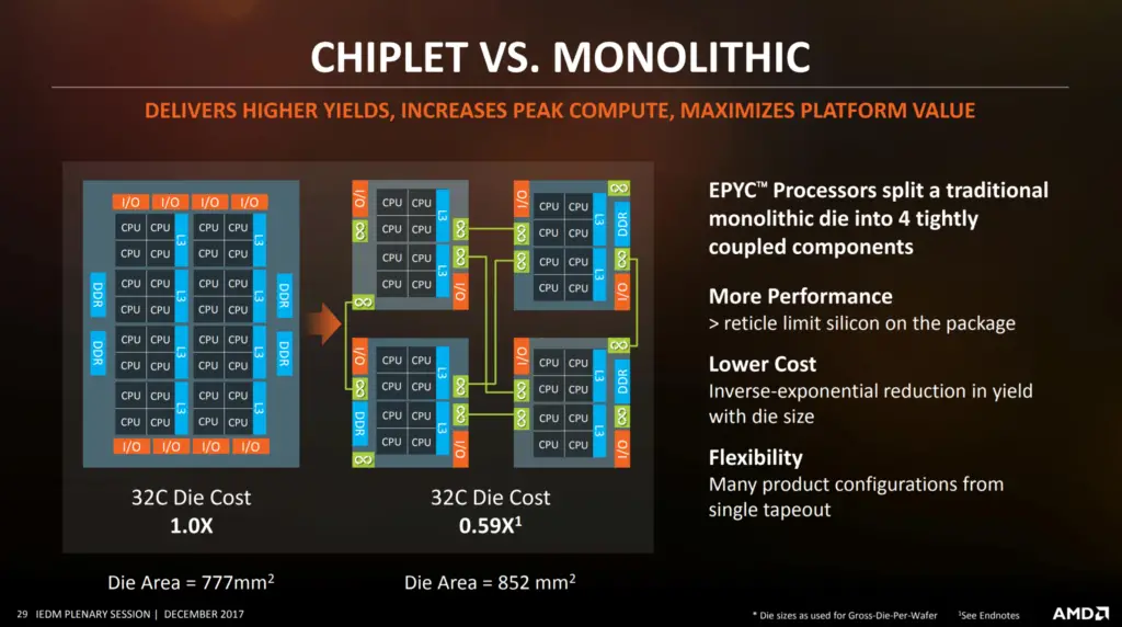
Each of the individual chiplets are 213mm² making the total die area 852mm². Su explains if they were to make an equivalent 32-core monolithic die, the die would be 777mm² which is incredibly uneconomical. The technique is not free and there is roughly 10% area overhead as well as some variations in latency. “But you are able to get a substantial reduction in die cost because you are on a different part of the yield curve for this technology†Su explains. Some of the added benefits of this architecture is the large amount of flexibility in the number of cores that you can sell, what you want to do with the large amount of I/O, and greater flexibility when sorting and binning the dies for various performance levels.
“I call this just the very beginning of multi-chip architectures. I think this is the first incarnation. We spent a lot of time in thinking on whether this is the right time to introduce this into a high-volume application. The thought process was, again, the packaging technology had matured, the silicon technology is mature, and together this would be a way to break existing constraints of Moore’s Law.†Su concluded.
Fixing The Memory Issue
Su sees similar opportunities with 2.5D packaging. Over the last decade, memory bandwidth failed to keep up with the processing power resulting in a lot of power being wasted on things that are other than computation. AMD hopes to remove this bottleneck. Su gave an example of high-bandwidth memory (HBM) they started utilizing in their graphics cards as early as 2015. “The issue here is not technology. The issue here is how do we manufacture it such that the cost is under control.†Su added.
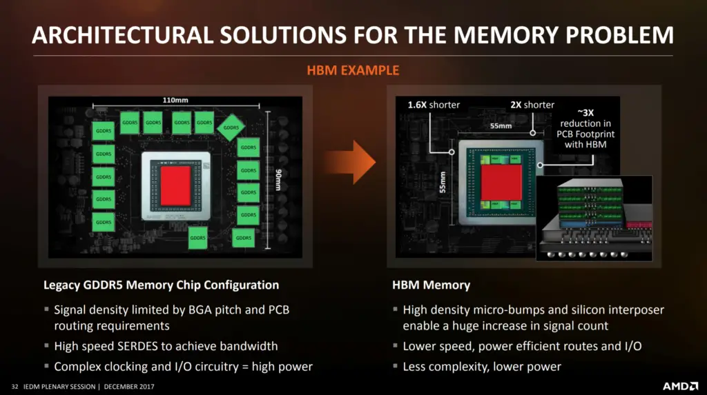
Not only does the footprint gets reduced, but the overall complexity is also reduced, consequently reducing the power required and increasing the bandwidth possible.
3D Stacking
3D is still the subject of research and has even started making its way to some low volume applications but has not reached high-volume manufacturing for high-performance devices. Moving to 3D means the memory dies are moved from not only the board to the chip, but directly on top of the processor die. Su noted “That in some sense is aspirational, but quite achievable given some of the research that’s going on in TSVs and other areas.â€
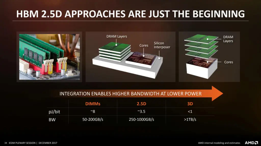
This approach reduces the power per bit by a significant amount as well as increases the bandwidth by a very large amount in experimental solutions. “We think this is a very promising forward step and something to look at for the next five plus years in terms of processor integration,†Su said.
Full 3D Stacking
Su’s ambitious vision didn’t stop with 3D stacking. She proceeded to explain a concept she called “full 3D stacking†whereby AMD would be able to stack the GPU on top of the CPU along with the HBM and NVRAM all together to form a “superchip†of a sort with incredibly high bandwidth and I/O communication between the data, the CPU, and the GPU.
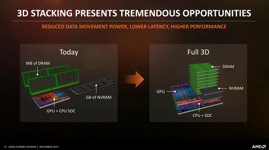
“I think technologically we can likely find a way to make it happen. What we have to work on as an industry is the cost and economics of this solution as well as the software and the ability for the software to really utilize those new capabilities.†Su added.
Those new solutions will become a necessity as the gap between computing power and bandwidth grows. Su believes these solutions will provide AMD with a step-function improvement as the industry moves forward.
The idea is not new but it was not previously proposed with as much seriousness in the HPC domain due to many of the challenges involved in commercializing the concept and dealing with many of the practical issues. It goes without saying that there are serious problems with those solutions such as heat dissipation and cooling. Following her speech, an attendee from Nvidia also asked her about the heat problem. Su believes many of those problems can be solved or mitigated with clever designs.
AMD is not alone in pursuing this approach. At this year’s conference GlobalFoundries also presented a paper where they proposed stacking the CPU directly on top of the SRAM. A number of methods were proposed and demonstrated for the removal of heat.
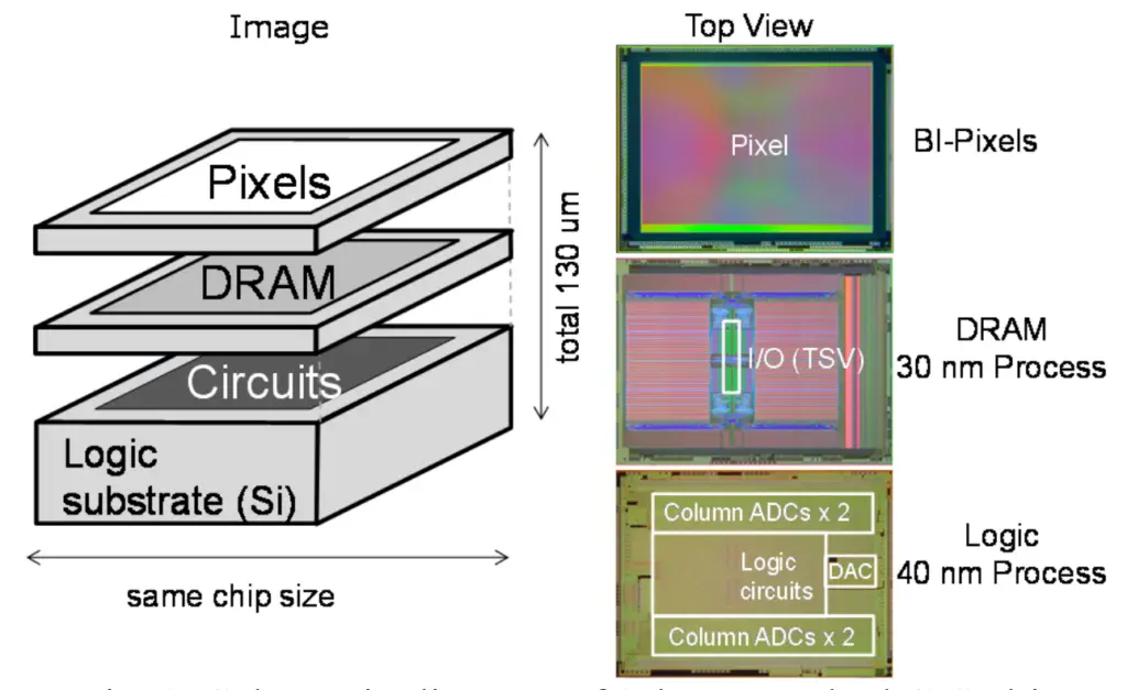
Other companies such as Sony even presented an actual product they developed – a 3-layer CMOS image sensor (CIS) sandwich chip consisting of stacked Pixel-DRAM-Logic with through-silica vias (TSVs).
Heterogeneous Architecture
Looking at the current system architecture, there is a large ongoing debate about what’s going to be the primary compute node in the future. Whether it will remain the CPU or move to the GPU, custom ASICs, or an FPGA. “I think from my perspective, it’s all of the above,†Su said.
AMD believes that in the future workloads will become increasingly diverse and no one type of design would be able to attack every problem. “In the legacy world, the CPU was the center of everything.†Su said. But in the future heterogeneous architectures will take on a much more prominent role.
Su believes that there is a lot of opportunity in not only maintaining the rate of performance and efficiency but also accelerating the performance curve over the next ten years. “What I would like to say is that there is an opportunity to really bring in all of the conversation around 2.5D integration, 3D integration, multi-chip architectures, memory integration, and different types of memory so that we re-architect the system in a way that each of the components are able to get as efficient as possible.â€
–
Spotted an error? Help us fix it! Simply select the problematic text and press Ctrl+Enter to notify us.
–