
IEDM 2017: AMD’s grand vision for the future of HPC
Barriers
Su identified a number of barriers that the industry will have to confront in the next decade.
Power
Power has become the first and foremost barrier required to take into consideration when designing future processors. Over the long haul the industry has been able to increase the power that the system can cool from around 150 W in 2006 to as much as 300 W today on modern GPUs through various cooling system innovations. Note that for server CPUs the figure is slightly less because they typically have higher density, making cooling more challenging.
“What you find with that increased thermal power is that you can’t increase the power indefinitely. At some point you are not going to be able to cool the system.†Su noted. AMD expects this area to continue to improve but at a much slower rate in the future.
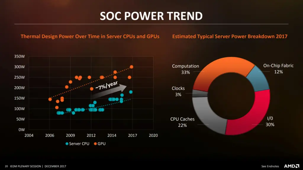
A growing problem is the fact that on a modern microprocessor, the power is distributed across many different areas. “Ideally, you want to spend all your power on computation. […] But because of all of the complexities, we are spending quite a bit of our power on idle, off-chip communications, and caches. Therefore the effect of the additional power on computation is not as direct as we would like it to be.” Su said.
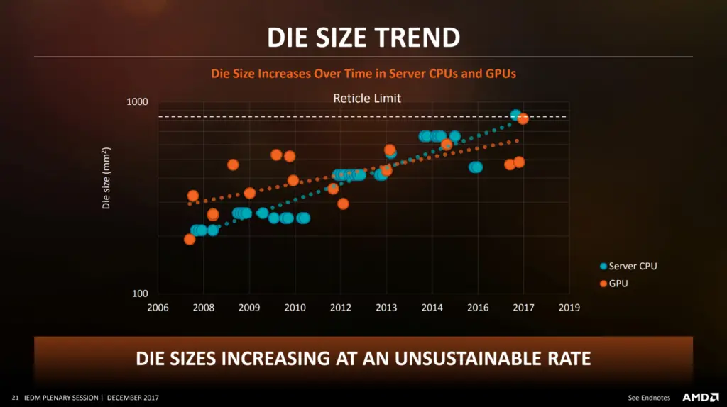
Die Size
While transistors keep getting smaller, logic designers have gotten an increased appetite for larger dies in order to add more features. In recent years, the demand for larger dies has grown far beyond what’s possible on modern lithographic processes. In the early 2000s dies size of 100-350 mm² was the range for the larger dies. Today, we see dies as large as 500-800 mm² on the largest high-performance chips. What we can observe is that we are very quickly reaching the reticle limits of what lithography can provide us. Alternative approaches will have to be considered in the future if we want to continue and utilize a large amount of transistors.
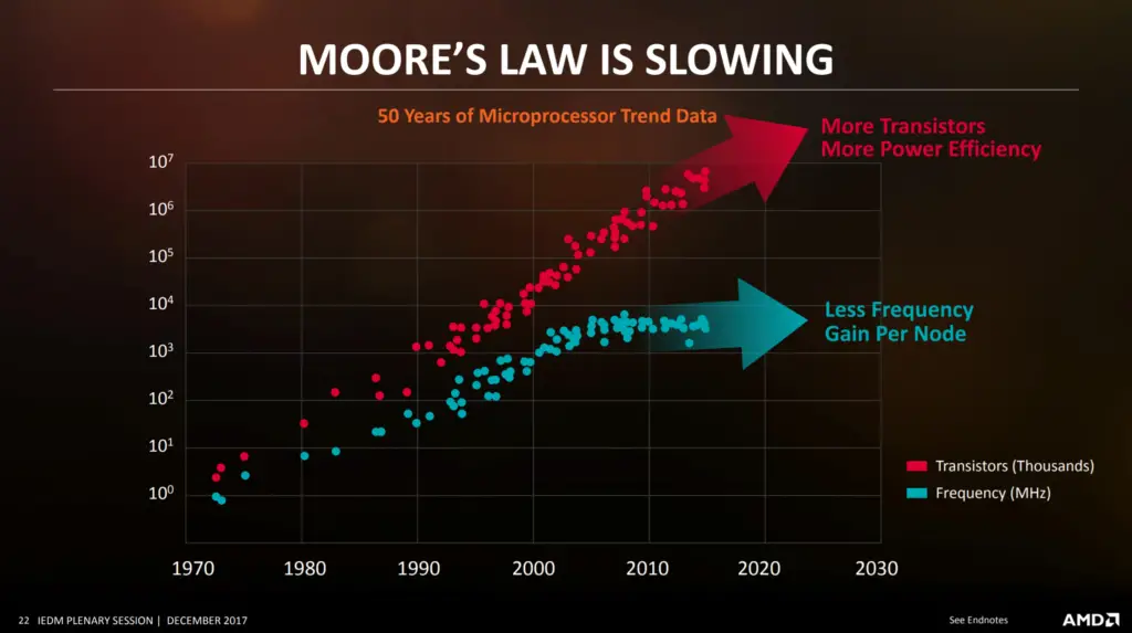
Moore’s Law
While Moore’s Law still marches on, we are not getting any more frequency gain. And while there is still power efficiency gains, there are limits as to the voltages that are acceptable in terms of liability.
The real problem Moore’s Law is facing is cost. The cost per yielded die area has been increasing quite substantially with recent nodes.
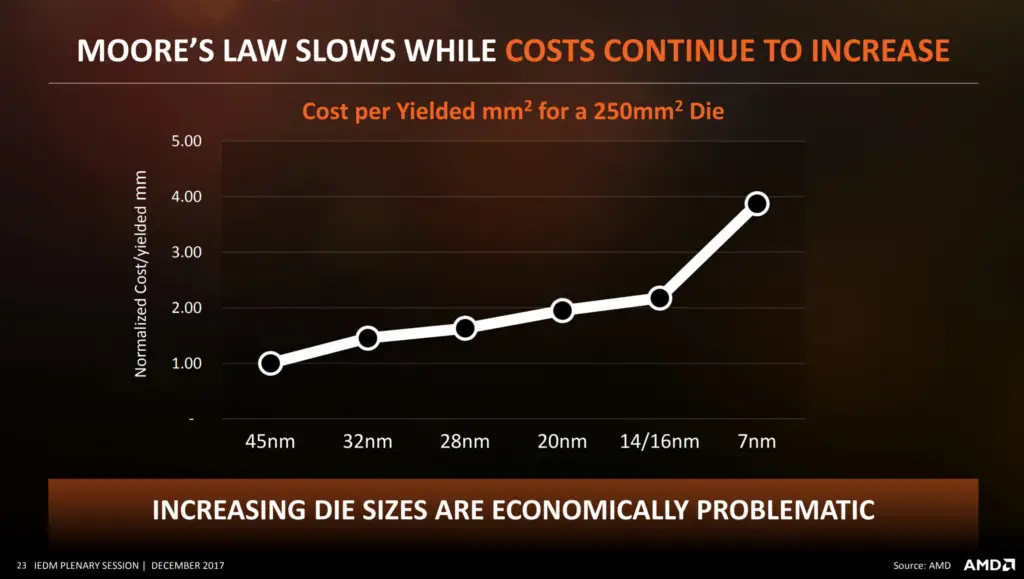
In fact, AMD reported close to 2x cost per yielded mm² for a 250mm² die. Interestingly enough I believe this is the first time any of the large semiconductor companies have reported on the cost increase for large dies on recent nodes. The large jump in normalized cost for large dies can comfortably explain why a company such as Intel has been taking its time moving to their 10nm node. It’s worth noting that moving an existing design from one node to the next results in a substantial die shrink. However, that quickly goes away when adding more core, caches, and other new large macro-blocks.
Memory Bandwidth
One of the major problems in modern microprocessor design is the communication between processing and memory. Su noted that this is a very important area for performance and it is an area that the industry has lost ground in an attempt to catch up with processing power.
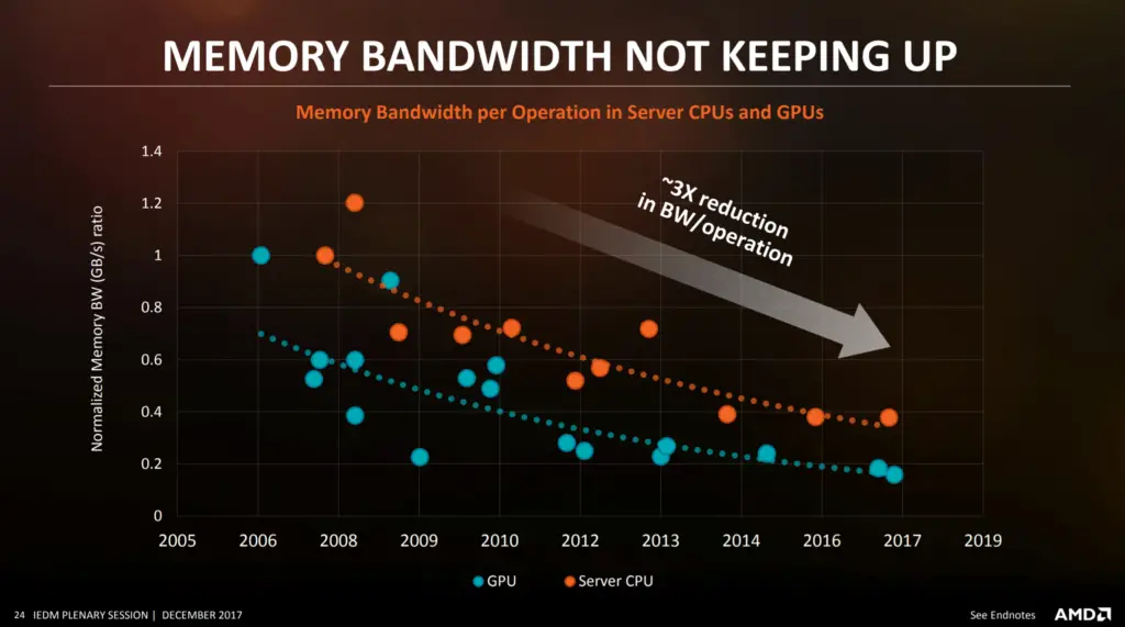
The graph above, shown by Lisa Su at her IEDM speech, plots the normalized memory bandwidth per computing operation. Over the last decade, we have actually lost major grounds. In other words, the GPU and CPU are increasing in performance at a much faster rate than the memory bandwidth. The inability to feed the processors with data fast enough continues to increase and as the gap widens, memory bandwidth will exceed in severity the other barriers in the future.
–
Spotted an error? Help us fix it! Simply select the problematic text and press Ctrl+Enter to notify us.
–