Japanese AI Startup Preferred Networks Designed A Custom Half-petaFLOPS Training Chip
Every year, 100s of the world’s leading vendors, universities, and research organizations come together at the annual Supercomputing conference Exhibits Hall. Over the years we’ve come accustomed to doing exhaustive visits to all the booths – especially the small ones with less-known names. While strolling through particularly small booths at one of the more remote corners of the show floor we came across the Preferred Networks (PFN) booth. In a booth measuring just a few square feet, we found one of the most interesting posters in the entire conference – a detail of PFN custom MN-Core AI training chip.
Founded in 2014, the Tokyo Japan-based startup has raised around $130 million, including $96.6 million from Toyota. The company primarily focuses on leveraging deep learning technology for heavy computing at the edge and IoT.
In-house Supercomputers
At its booth, we met Kei Hiraki, Emeritus Professor at The University of Tokyo. Professor Hiraki has been involved in the development of PFN’s MN-Core. Hiraki explained that PFN has been developing a series of private supercomputers in order to accelerate its own R&D of applications involving deep learning using a very large amount of compute power. In 2017 the company launched its first AI supercomputer, the MN-1. The system featured 1,024 Nvidia Tesla P100 GPUs achieving a peak compute of 1.39 petaFLOPS and 9.3 petaFLOPS of SP from the GPU. At the time, the MN-1 ranked 1st in Japan and 12th in the world on the TOP500 among industrial supercomputers. In July 2018 PFN enhanced the MN-1 by adding 512 additional Tesla V100 GPUs. The newer system, MN-1b, increased the compute power to 56 petaFLOPS of deep learning (tensor). Earlier this year PFN launched its largest supercomputer to date, the MN-2. Going into operation in July 2019, the system doubled the number of V100 GPUs and switched from PCIe cards to SXM2 modules.
| Preferred Networks | |||
|---|---|---|---|
| Computer | MN-1 | MN-1b | MN-2 |
| CPU Cores | 2,048 | 2,304 | 5,760 |
| GPU | P100 (PCIe) | V100 (PCIe) | V100 (SXM2) |
| GPUs | 1,024 | 512 | 1,024 |
| DL Performance | 19.1 petaFLOPS | 57.3 petaFLOPS | 128 petaFLOPS |
MN-Core, A 500-Watt MCP
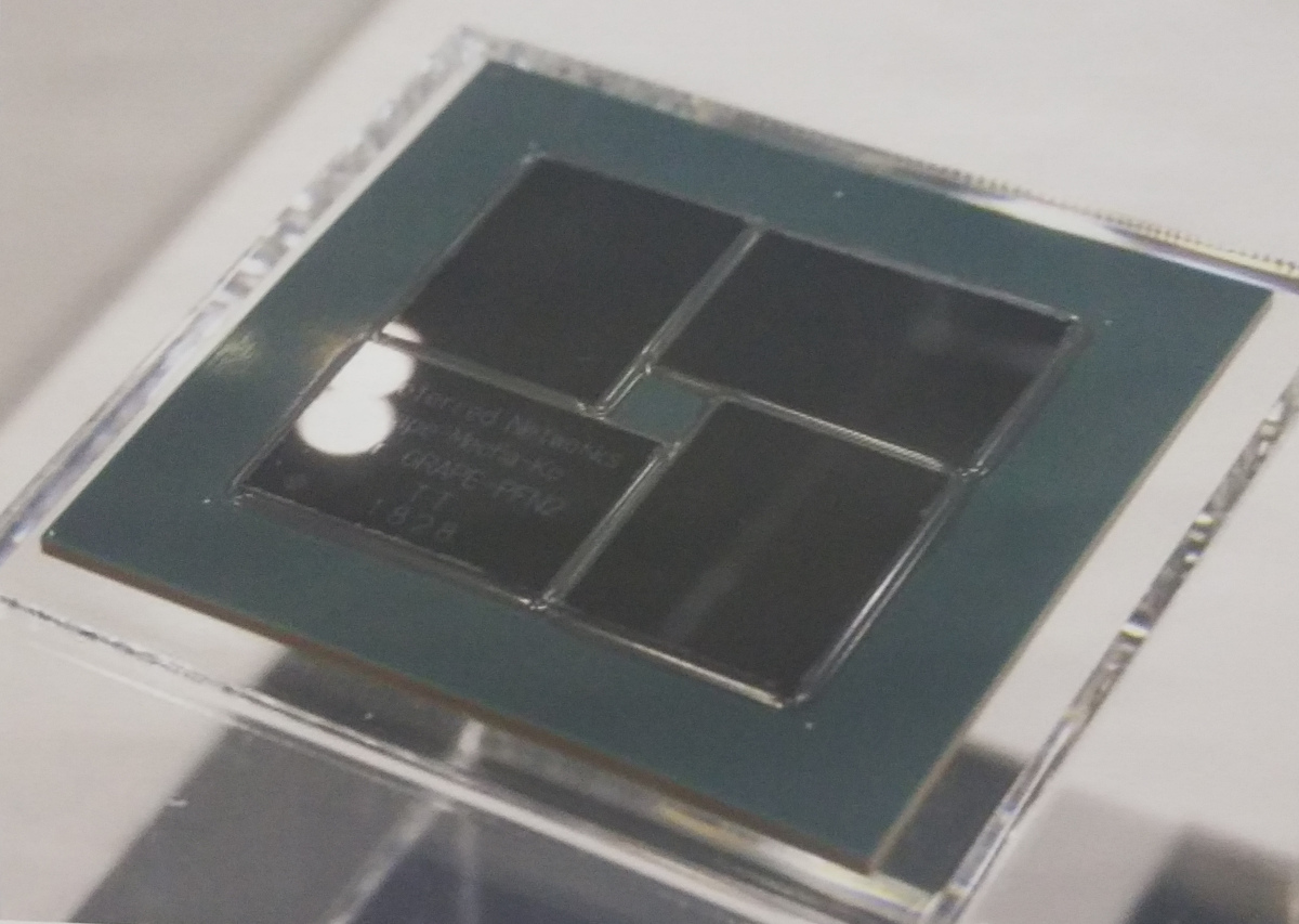
PFN next supercomputer is far more interesting. Professor Hiraki explained that PFN decided to develop its own proprietary deep learning accelerator with higher performance and more importantly a goal of achieving higher power efficiency. What they designed is a 500 Watt chip which Hiraki said is right at the limit of what’s possible to cool. The chip itself comprises four dies in a multi-chip package. The dies are fabricated on TSMC 12-nanometer process based on the company’s own design.
In the photo of the chip above, the word “GRAPE-PFN2” is engraved on the die. Although it’s unclear as to the reason for that engraving, it seems that some of the architecture was derived from the GRAPE-DR. It’s also worth pointing out that members of the Preferred Networks team previously worked on the GRAPE-DR physics coprocessor – including Professor Hiraki. The package itself is huge – measuring 85 mm by 85 mm. The dies are also incredibly large at 756.7 mm². At 500 W, the chip is capable of 524 teraFLOPS (half-precision). This gives them a compute power-efficiency of 1.05 TFLOPS/W which is what they were aiming for.
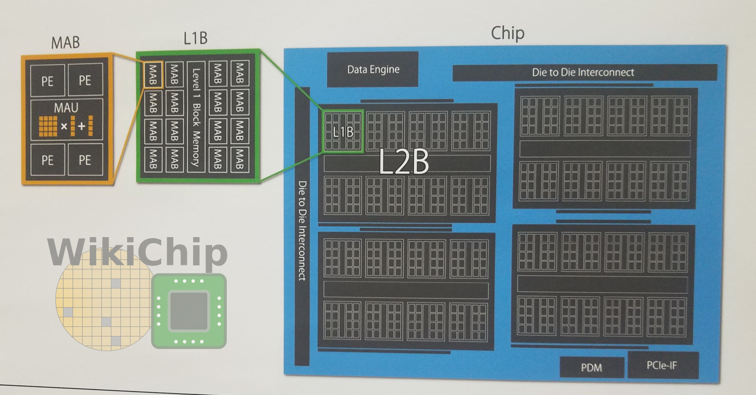
The architecture resembles that of the GRAPE coprocessor. The individual blocks are even named similarly and the overall operation is quite similar although it has been adjusted for training. There are DRAM I/Fs, PICe I/Fs, and four level-2 broadcast blocks (L2Bs). Within each L2B are eight L1Bs and a block memory. The level-1 block includes 16 matrix arithmetic blocks (MAB) as well as its own block memory. The matrix arithmetic units and four processing elements (PEs) make up a single MAB. In total, there are 512 MABs per die.
The individual processing elements pass the data to the MAU. The PEs incorporate an ALU and implement a number of custom DL functions that PFN specifically uses, although it is much more specialized than most other NPUs. The basic data type operation is 16-bit floating-point. Higher precision operation is supported by combing multiple PEs.
MN-3 Supercomputer
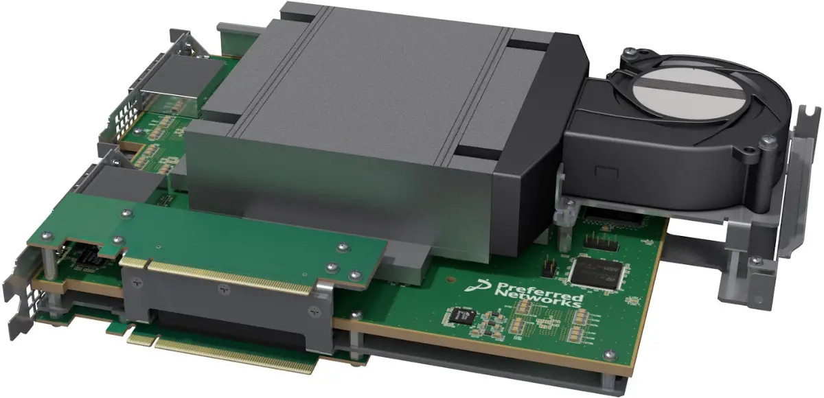
The chip itself sits on the MN-Core board, a custom PCIe-based accelerator board PFN designed. With a power consumption of 500 Watt and 0.55 V, there are almost 1,000 amps going through the board and the package which Professor Hiraki said posed a significant design challenge. The board itself is a x16 PCIe Gen 3.0 card which incorporates the MN-Core chip, 32 GiB of memory, and a custom-designed heatsink and fan. PFN estimated the card to consume around 600 Watts.
Four MN-Core boards are mounted in on the MN-Core server, a 7U rack-mount chassis. There is a dual-socket CPU in each server. Four boards allow them to reach 2 petaFLOPS of half-precision floating-point operations per second.
| MN-Core Board And Server | ||
|---|---|---|
| Board | Server | |
| MN-Core | 1 x Chip | 4 x Chips |
| Peak Perf (HP) | 524 TF | 2.096 PF |
PFN plans on stacking four of those servers per rack. Preferred Networks next-generation supercomputer, the MN-3, will be based on the MN-Core.

PFN, like may companies, has no plans on selling this chip. Their decision to publically talk about it means we get a unique glimpse at the side of the semiconductor industry we don’t normally get to see. PFN MN-Core chip and supercomputer will be used for its own R&D exclusively. PFN expects the MN-3 to have around 300 racks which work out to 4800 MN-Core boards. This translates to just north of 2 exaFLOPS of half-precision floating-point operations per second. In terms of power, we are estimating the machine to come in at 3.36 MW which is incredibly low for this kind of performance. The 13 MW Summit, for example, reached 1.88 exaOPS. The MN-3 is planned to go into operation in 2020.
We have seen hyperscalers such as Google and Amazon developing custom neural processors for their own cloud servers. A similar trend is emerging in the industry with companies such as Preferred Networks designing its own NPU. The common theme remains the same – companies that are capable of developing their own hardware are designing their own chips in order to have a unique, differentiating, technological advantage. Less than a handful of AI hardware startups are currently shipping inference chips and no startup is shipping a training chip. The lack of commodity specialized training chips opens up a unique opportunity for companies by exceeding the performance and power efficiency of current top-of-the-line training GPUs. The landscape might change as more commodity training chips start entering the market.
–
Spotted an error? Help us fix it! Simply select the problematic text and press Ctrl+Enter to notify us.
–

