VLSI 2018: Samsung’s 2nd Gen 7nm, EUV Goes HVM
Overview
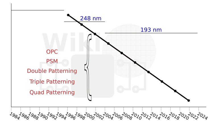
Starting around 2004, the industry slowly switched to 193 nm lithography. But the critical feature sizes have long dropped below this wavelength. To pattern such small features, the industry employed a slew of lithography tricks such as optical proximity correction, double patterning, and even quad patterning.
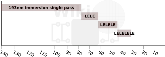
Samsung has been using a double patterning technique known as Litho-Etch-Litho-Etch (LELE) once features dropped below the wavelength limits. Recently, for their 10nm technology, they dropped under the double patterning limit forcing them to use triple patterning (Litho-Etch-Litho-Etch-Litho-Etch or LELELE). Finally, at this conference, Samsung unveiled their 8nm which pushes patterning further to LELELELE (Quad).
Under LELE you start out with a substrate, the device layer, and the hardmask. The layer is then split into two masks. Suppose we want to achive a minimal metal pitch of 64nm (similar to Samsung’s 10nm).

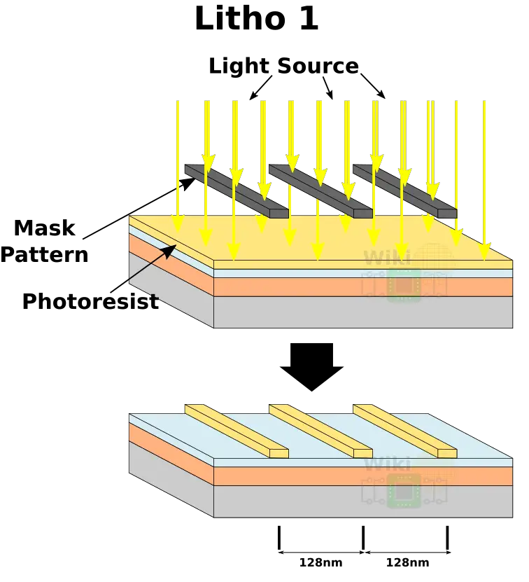
We would then apply the photoresist and expose it to light over a mask in order to get the desired pattern. Since our desired minimal metal pitch is 64nm, we can start with a 128nm pattern pitch.
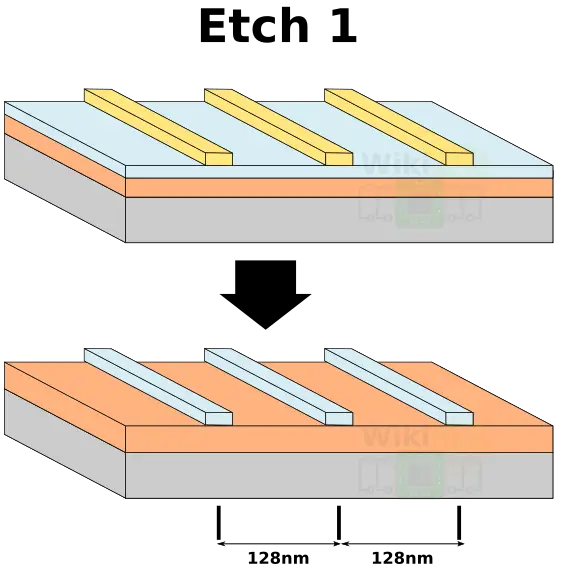
We then transfer the pattern onto the hardmask which will be used for subsequent steps serving as an ad hoc mask.
Now we can shift the pattern and repeat the process with another set of patterns and photoresist using the same 128nm pattern pitch.
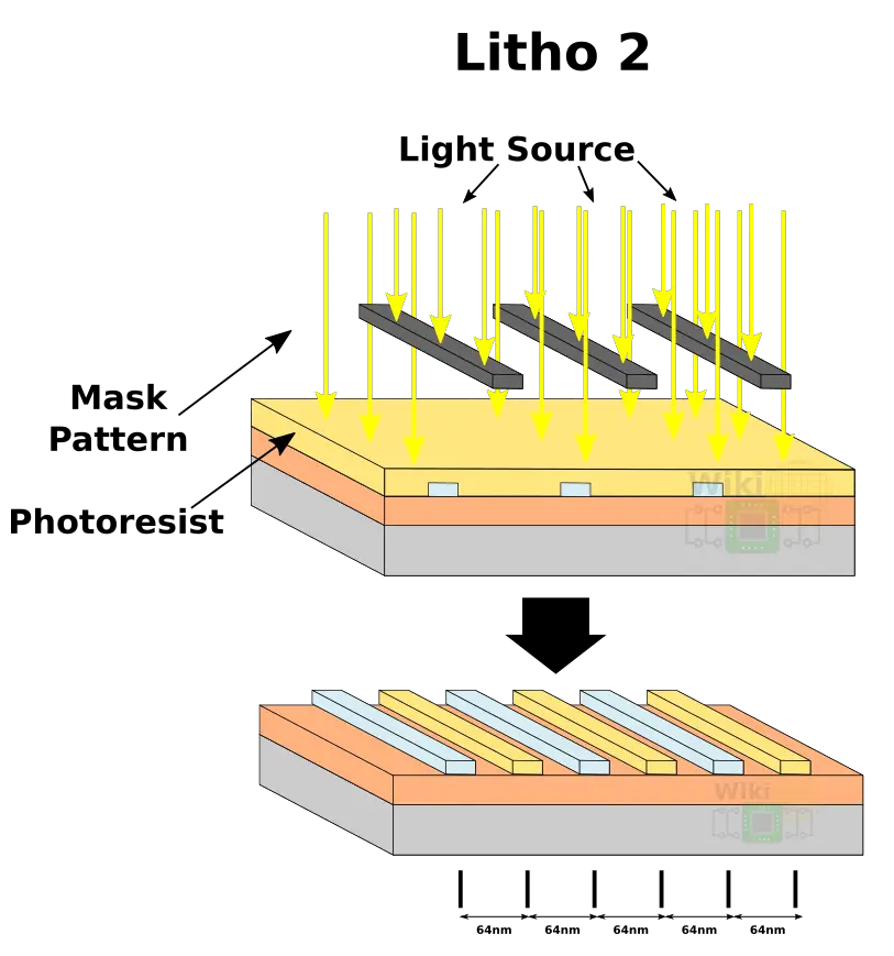
We finally use the hardmask and resist as an etch mask for the underlying device layer.
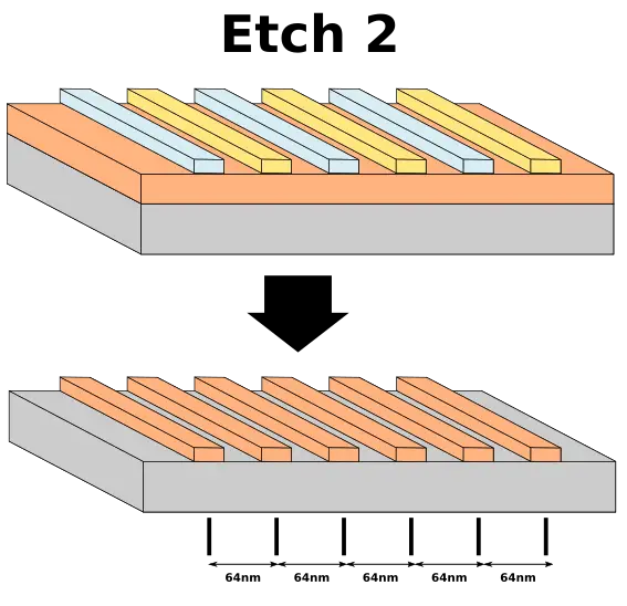
Following the second etch we’re left with the desired pattern where the minimum pitch is achieved is the desired 64nm for this process. This technique has been extended by Samsung for LELELE and LELELELE though the addition of another litho and another etching step allowing them to go to sub-44nm pitches.
–
Spotted an error? Help us fix it! Simply select the problematic text and press Ctrl+Enter to notify us.
–
