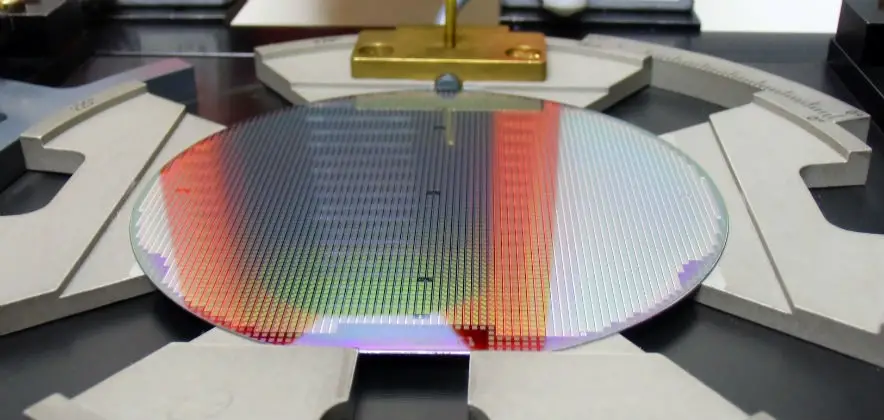
Samsung Details 5nm and 4nm; Adds 8LPA, 5LPP, and 4LPP Nodes; Readies 3nm GAA For Next Year
Over the past few years, Samsung Foundry has been putting considerable effort into expanding its foundry offering. The company is pouring significant investment in an effort to win customers from its rival foundry, TSMC. As part of this move, Samsung has invested heavily in EUV starting with their 7-nanometer node which ramped in early 2019.
The 7-nanometer node "family" has been furthered enhanced over the last couple of years through a series of node branches that scaled area or improved the device characteristics. Samsung's latest advanced node is the 5nm node, 5LPE. The process entered mass production late last year with chips already making their way into the latest smartphones.

This article is reserved for our subscribers.
In addition to our usual, free, coverage of cutting-edge semiconductor technologies and state-of-art chips, a subscription offers exclusive, early access to additional articles such as this one. Learn more here.

