AMD’s Zen CPU Complex, Cache, and SMU
Caches
L1 Cache
For the level 1 cache, AMD uses 8T bitcells. There are actually 5 different size variants of their 8T cell which are used in various areas of the core (e.g., Instruction, Data, etc.). The instruction cache is 64 KiB 4-way set associative. The data cache is 32 KiB 8-way set associative with a write-back policy.
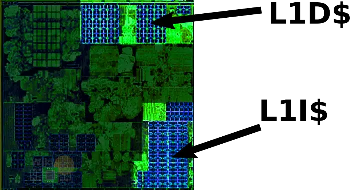
The data cache policy was changed from prior designs where AMD had used a write-through policy. It is ECC-protected and there are additional bits that were added in order to implement single error correction with double error detection (SEC-DED) in order to not necessitate column muxed writes. Because of this, the L1 sits on the same core VDD domain instead of the dedicated SRAM supply (i.e., VDD,M) which simplifies timing and complexity but might require a voltage boost above the core supply. pMOS capacitors are used to boost the write word line with configurable JTAG signals, allowing up to three different boost levels to a virtual VDD (corresponding to a group of WWL drivers) based on the capacitor’s size. The design is quite similar to what AMD has done with Excavator but with a number of enhancements. Boost-enable input bits come from the system management unit (SMU, discussed later). If the boost bit is asserted (e.g., at low voltages), on writes, the WWL will be bumped above the core supply voltage. To ensure proper reliability, the SMU will not boost above VMAX.
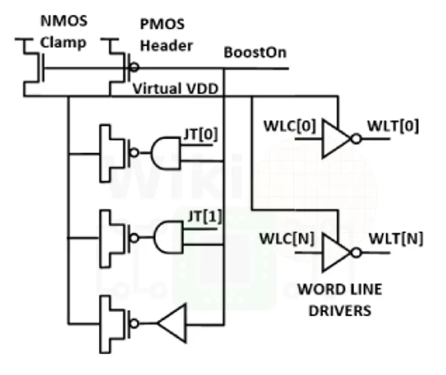
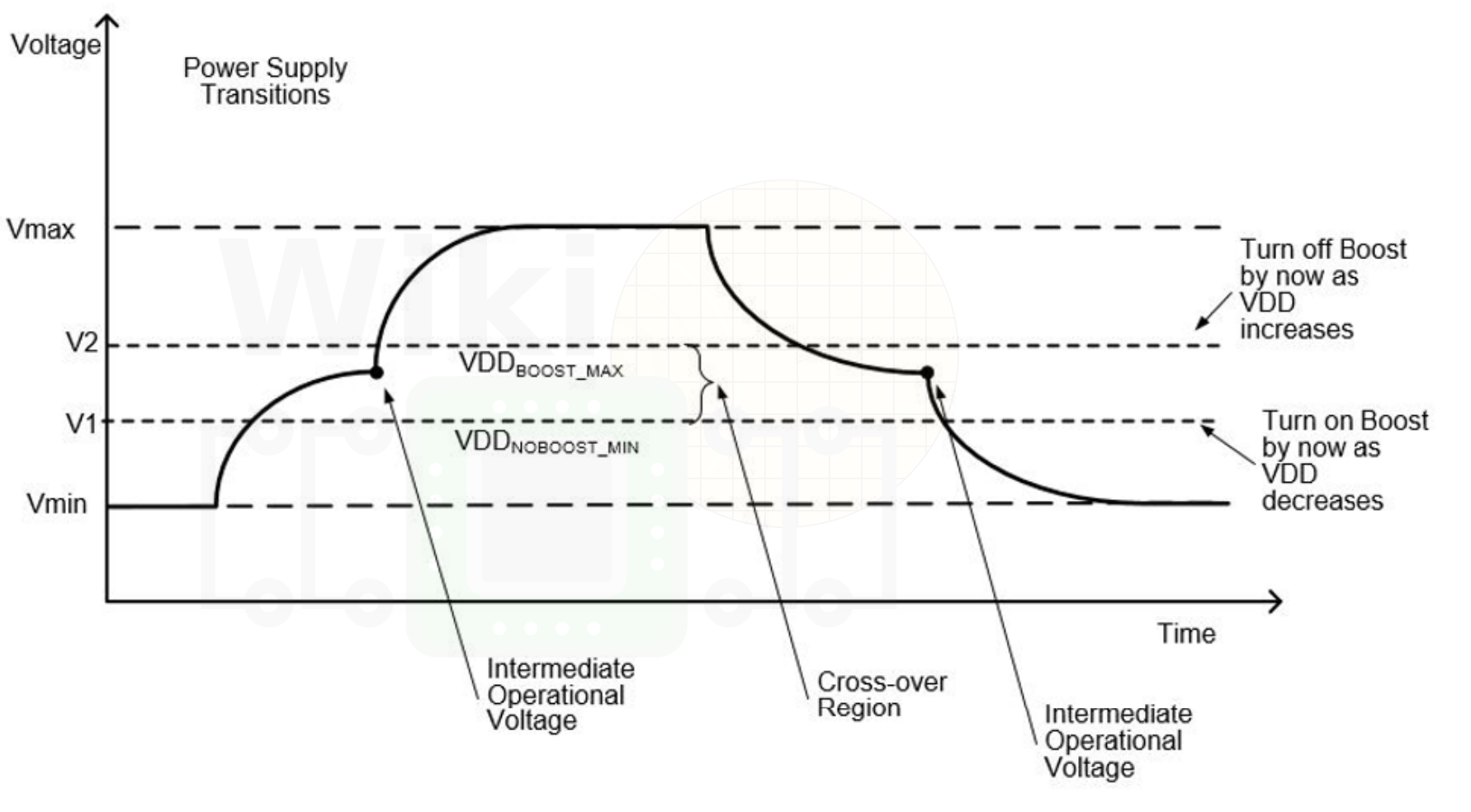
There are a couple of caveats to this design. In Excavator, AMD had to disable the macro when the core was transitioning to FMAX/VMAX. In Zen, this is avoided through the use of a two-stage voltage transition. Upon switching to FMAX, the core will transition to an intermediate (V1) voltage state where the WWL boost is no longer required and if it’s already enabled, it will not exceed VMAX. In this stage, if the boost bit is asserted, it is de-asserted, allowing the core voltage to boost to its final state without ever exceeding WWL VMAX. The boost mechanism does affect the write timing meaning read after write (RAW) hazards exist for the same address. Zen avoids stalls by implementing a bypass MUX on the output for RAW to the same address. The previous cycle’s input is selected over the usual output in those occurrences.
L2 Cache
The level 2 cache is 512 KiB 8-way associative and strictly inclusive of the first level cache (both instruction and data). The L2 has a bandwidth of 32 bytes per cycle to the L1/L3 in each direction for a single core or 128 bytes per cycle in each direction for the four cores in the CCX. L2 probes can invalidate instruction and data cache lines or be replaced based on a least recently used (LRU) replacement policy. Three custom SRAM macros make up the L2 cache: State, Tag, and Data.
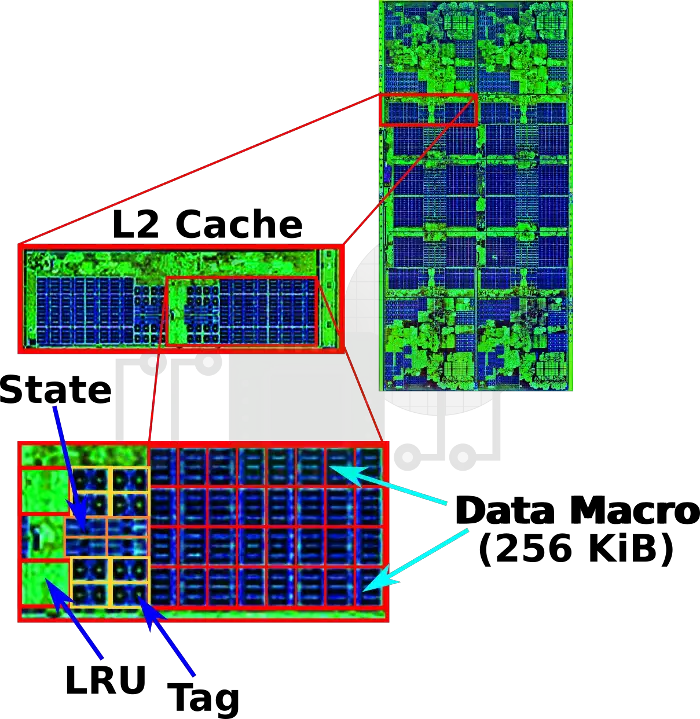
The entire L2 is supplied from the VDD,M voltage domain. High-current 6T bitcells are used for the Tag and Data macros for density whereas the State macro uses an 8T bit cell for the added read and write bandwidth. Parity checks are done for all ways during state and tag matching whereas single error correction with double error detection (SEC-DED) is conducted on victim and hit ways. Additionally, L2 read data is protected by DEC-TED which is said to have no performance penalty and only roughly 6% increase in switching capacitance over SEC.
L3 Cache
Consuming the largest portion of the complex at 16 mm², the level 3 cache is shared by all the cores. The L3 consists of four slices of 2 MiB per core, interleaved by the low order address.
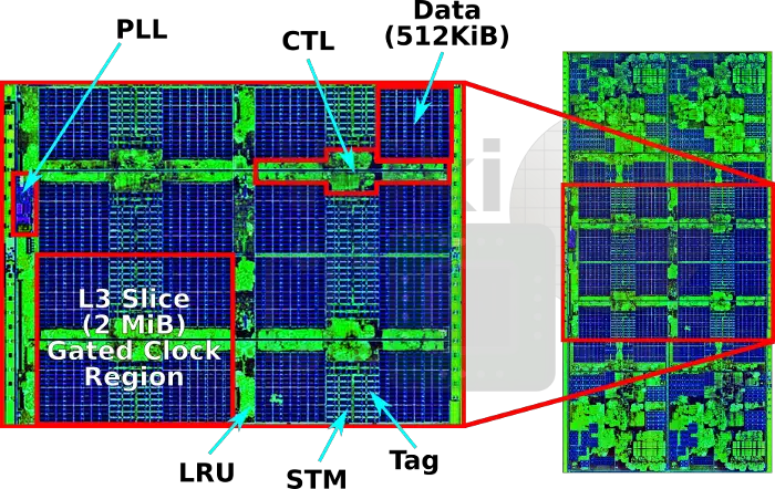
Annotated on the picture above in the left corner is the PLL which is used to generate the clocks for the L3 as well as all the cores, keeping the L3 interface with the cores fully synchronous. Also shown in the picture above is an individual slice which is made of four clock regions. Each one of those regions is capable of being independently gated depending on the activity. This is said to significantly contribute to Zen’s overall power saving. Since the cores sit on their own voltage domains with potentially different voltage levels, there is a level shifter FIFO at each interface to handle the mismatch.
The L3 is filled with L2 victims. There are also special shadow tags found in each slice which duplicate the L2 state/tag entries for indexes in that slice. On an L2 miss or an external CCX probe in the case of multiple CCX configurations, those shadow tags are checked in parallel to the L3 checks in order to alleviate actual L2 bandwidth. The CCX itself was designed such that the L3 acts as a crossbar for each of the four cores.
System Management Unit
As briefly mentioned earlier, the system management unit (SMU) is tasked with the job of continuously sampling sensory data and making rapid corrections to various circuits on the chip. One such example is the control of the boost circuit we detailed earlier. Additional tasks include voltage level control which is supplied as targets to the power supply monitors (PSMs), C-state boosts, thermal management ensuring the chip does not exceed the spec temperatures, and electrical design current management which ensures the current draw does not exceed the specs of the external voltage rails. The SMU itself uses the Scalable Control Fabric (SCF) plane of the Infinity Fabric to communicate with all the functional blocks on the chip.
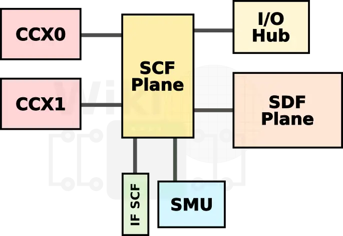
The SCF itself has a dedicate Infinity Fabric InterSocket (IFIS) SerDes for communication across dies. This also extends to other chips in a dual-socket configuration.
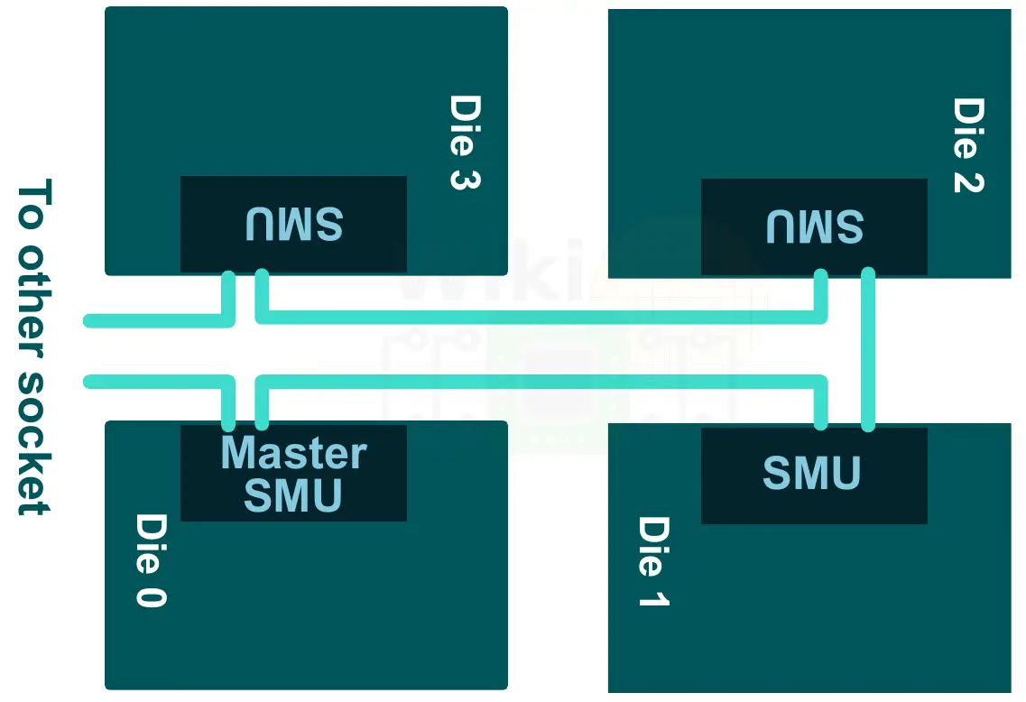
The SMU consists of two operational loops. All operations are first managed locally within each die by the local SMU in a fast control loop and then globally in each socket by a single Master SMU in a slower loop.
–
Spotted an error? Help us fix it! Simply select the problematic text and press Ctrl+Enter to notify us.
–
