
A Look at NEC’s Latest Vector Processor, the SX-Aurora
VPU
Ideally, the majority of compute-intensive work should be happening in the vector processing unit. The VPU has a pipelined control logic. The scheduler has a dedicated port to a complex operation execution unit and to the vector parallel pipelines (VPP). The complex operation unit deals with high-latency operations. The SX-Aurora doubles the number of VPPs. Each VPU now has 32 identical VPPs. The VPP has an eight-port vector register, 16 mask registers, and six execution pipes.
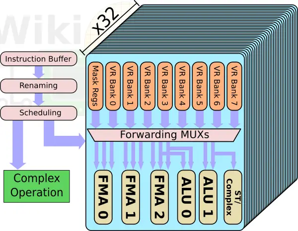
Note that the effective number of pipelines executing each cycle is actually four. That is because two of the execution units are MUX’ed on the same read ports. The SX-Ace only had two FMA units. With Aurora, NEC added a third one. The VPP is designed such that all three FMAs can execute each cycle – each one can be independently operated by a different vector instruction. Every FMA unit is 64-bit wide and can support narrower packed operation such as 32-bit for double the peak theoretical performance. If this was a standard CPU core, it would be as if it had 96 SIMD units. It’s worth pointing out that NEC’s SX architecture has a very wide vector length the size of 256 elements with each element being 8 bytes (i.e., 2 KiB). Therefore a single vector operation requires eight cycles to complete by a single FMA pipeline across all 32 VPPS. There are 64 architectural registers (i.e., 128 KiB/core) and 256 physical in total. The reason for the narrower SIMD units compared to contemporary designs such as AMD’s Zen and Intel’s Skylake which have 128-bit and even 512-bit SIMD units is to be able to take advantage of temporally parallel operations in order to hide memory access latencies.
Feeding the VPU
Historically, NEC has spent a lot of effort on ensuring their vector cores are well fed. Insufficient bandwidth will quickly bottleneck the VPUs which will prevent them from achieving their high FLOPs.
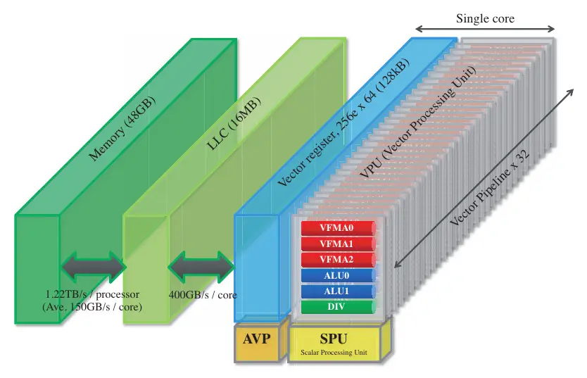
Consider the SX-Ace which was introduced in 2013. In the SX-Ace, there were four cores with 16 VPPs per VPU with 2 FMAs per VPP. Operating at 1 GHz, this translates to 64 gigaFLOPS per core or 256 gigaFLOPS in total. The four cores were attached to a crossbar which had an aggregated bandwidth of 256 GB/s which was connected to the 16 memory channels. Supporting DDR3-2133, the chip also had an aggregated memory bandwidth of 256 GB/s. In other words, the system bytes/flop ratio is 1.
| SX-Ace | ||||
|---|---|---|---|---|
| GF/core | GF/system | XBar B/W | Memory B/W | System B/F |
| 64 gigaFLOPS | 256 gigaFLOPS | 256 GB/s | 256 GB/s | 1 byte/FLOP |
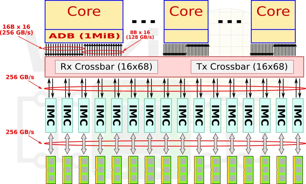
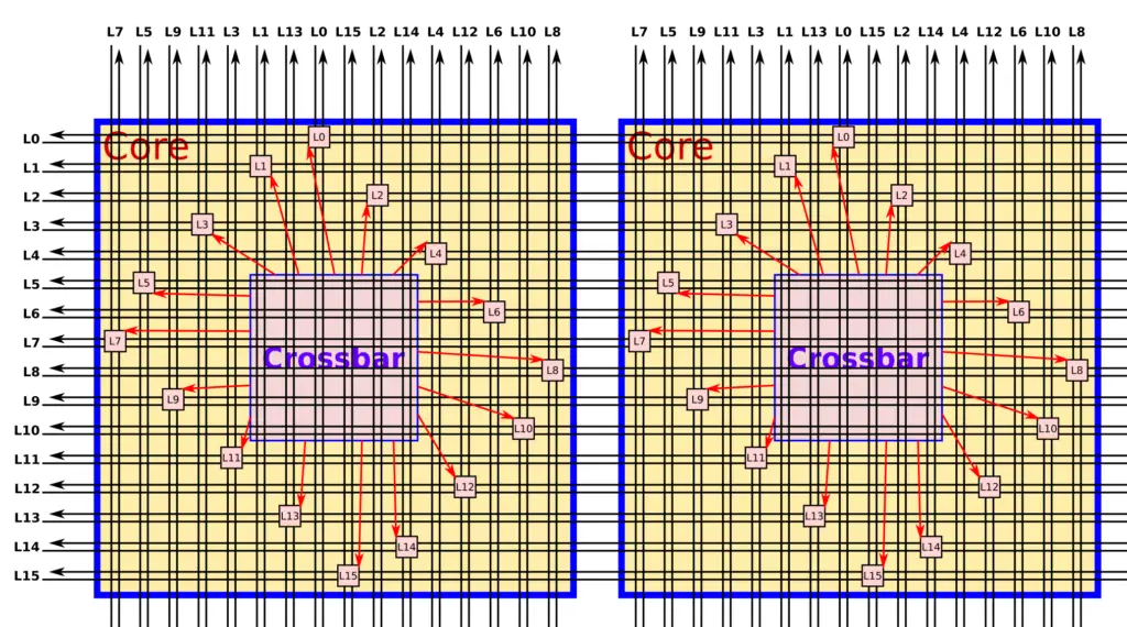
In the SX-Aurora, NEC quintupled the FLOPS per core from 64 GF to 307.2. They got rid of the 1 MiB assignable data buffer (ADB) and instead added a 16 MiB shared last level cache which is inclusive of both the L2 and L1. The cores and the caches are connected over the mesh which is a 16-layer 2D mesh network designed to maximize bandwidth by minimizing physical transfer distance.
The request and reply crossbars can, each, issue up to 16 requests per cycle. At 16B/request, we are looking at 410 GB/s at 1.6 GHz (max operating frequency of the SX-Aurora) each. On the memory subsystem side, the last level cache has an aggregated bandwidth of 3 TB/s. The caches are sliced into eight 2 MiB chunks which consist of 16 memory banks each. The LLC interfaces with the IMC at 200 GB/s per chunk (1600 TB/s in total) and those provide a memory bandwidth of 1.22 TB/s through it’s 6 HBM2 modules.
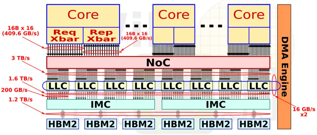
Although NEC didn’t quite match the bytes/FLOPs ratio of the prior system, compared to contemporary designs, the SX-Aurora achieves much better memory bandwidth to compute power.
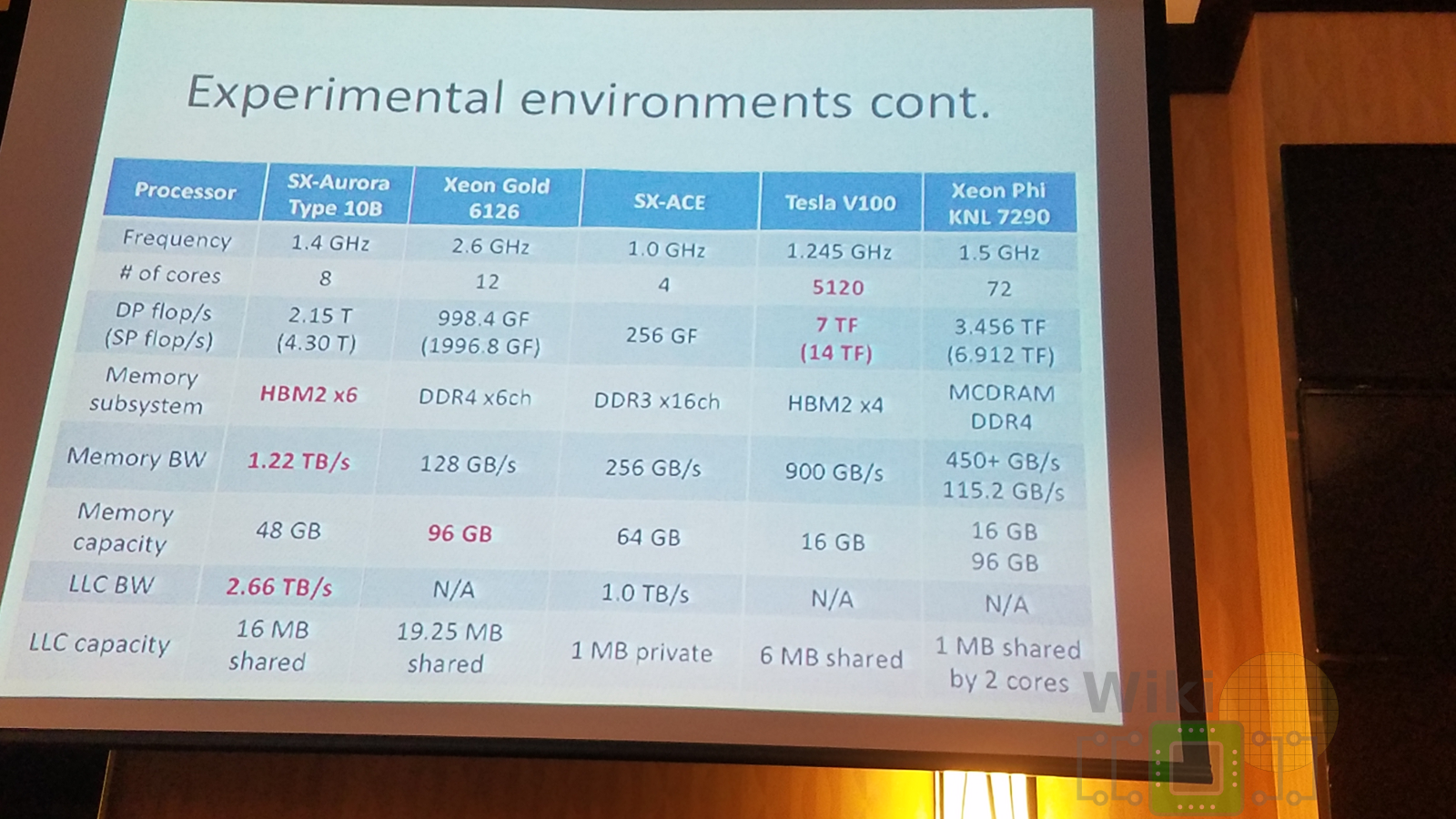
| Processor Comparison | ||||
|---|---|---|---|---|
| Processor | VE 10A | Platinum 8180 | Tesla V100 | |
| Frequency | 1.6 GHz | 2.3 GHz | 1.25 GHz | |
| Cores/EU | 8 | 28 | 5120 | |
| Perf/core | 307.2 GF | 73.6 GF | 13.67 GF | |
| Perf/socket | 2.46 TF | 2.06 TF | 7 TF | |
| Max Mem | 48 GiB | 765 GiB | 16 GiB | |
| Memory | 6 x HBM2 | 6 x DDR4 | 4 x HBM2 | |
| Memory B/W | 1.22 TB/s | 128 GB/s | 900 GB/s | |
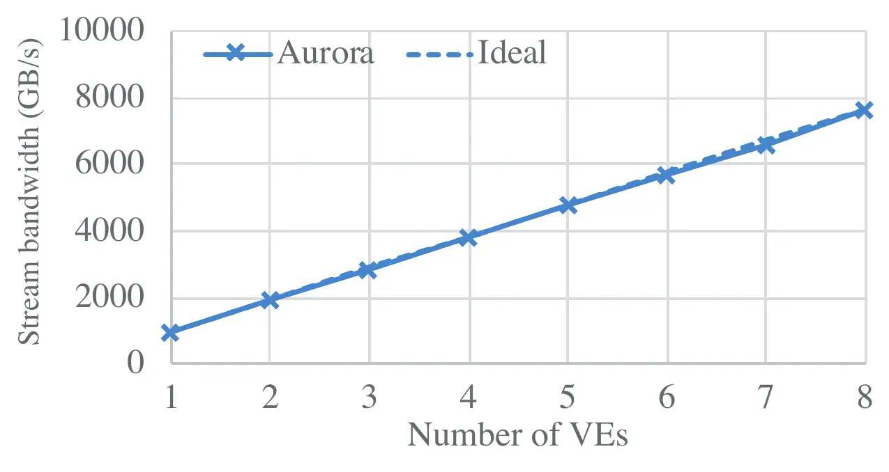
At the NEC Aurora Forum at Supercomputing 2018, Kazuhiko Komatsu, Research Associate Professor from Tohoku University presented some of their benchmarks.
 |
 |
As far as memory scaling, NEC reports near-ideal scaling for Steam on the A300-8 system featuring eight accelerators. Likewise, on the Himeno benchmark which measures the performance of solving the Poisson equation by using the Jacobi iteration method, the same system exhibit very good scaling up to four vector engines. With five and more VEs, NEC reported that the overhead of the reduction calculation adversely affect scalability.
 |
 |
 |
The Package
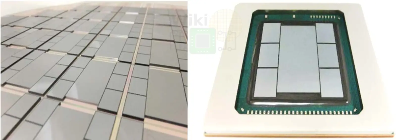
The key to the high memory bandwidth of the SX-Aurora is the packaging. The SX-Aurora chip uses six HBM2 stacks. Those are either 4 Hi or 8 Hi stacks. The chip utilizes TSMC’s second-generation chip on wafer on substrate (CoWoS) technology with NEC’s implementation developed in collaboration with TSMC and Broadcom. It’s worth pointing out that this chip became the world’s first to utilize six HBM2s.

Due to the heat generated by the SX-Aurora, the package has no heat sink. A stiffener is used instead to improve the mechanical reliability of the package. To remove the heat as quickly as possible to prevent the HBM2 modules from throttling, contact is done directly with the die.
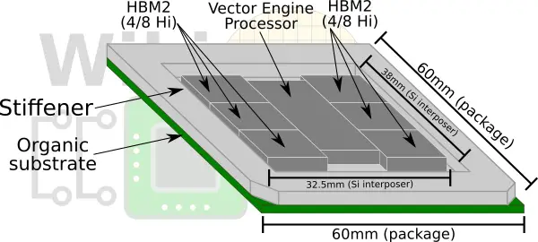
TSMC’s first-generation CoWoS technology was used with Si interposers of up to ~800 mm². The interposer used for the SX-Aurora is very large – 32.5 mm x 38 mm (1235 mm²). It exceeds the size of a reticle, meaning fabricating it cannot be done with a single set of masks.
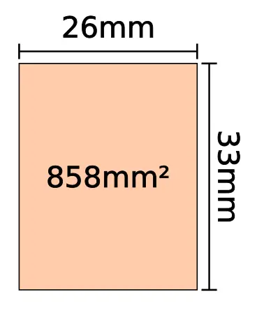
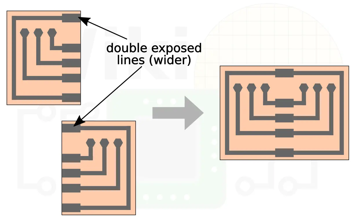
With second-generation CoWoS, TSMC extended this to 1200 mm². Although originally qualified for 1,200 mm², TSMC has since extended it to 1,700 mm² (note that Volta gets close to that). To solve the reticle size restriction, TSMC uses a technique called mask stitching. Two masks are combined together with each slightly overlapping each other.
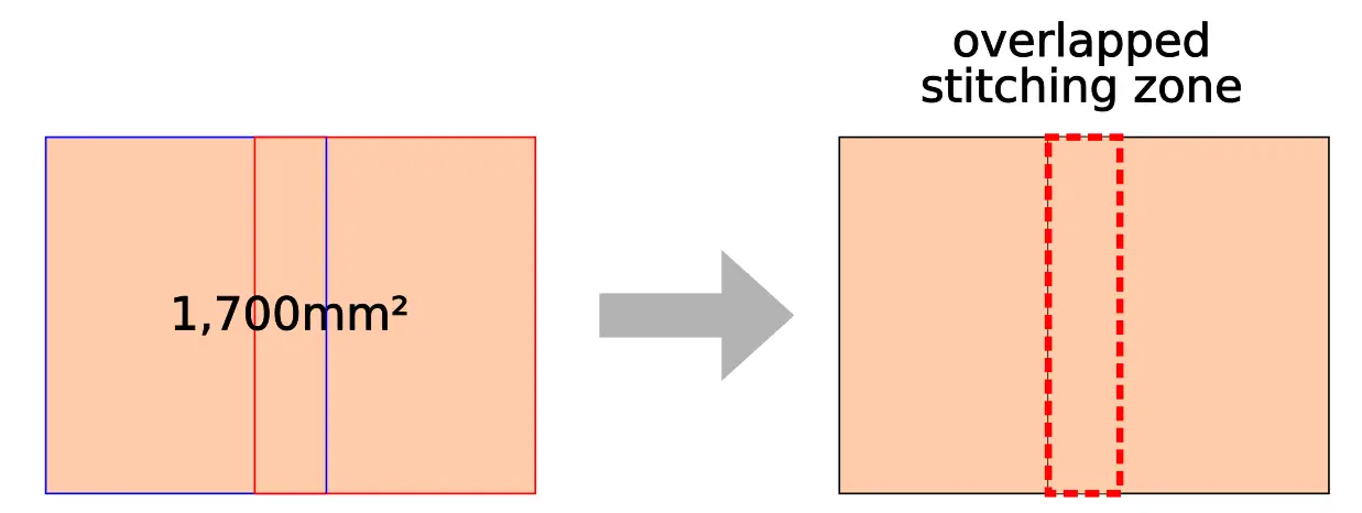
The overlapped region of the redistribution layer (RDL) interconnect lines are identical for both masks. TSMC reports negligible resistance from the dimension variation in the overlapped stitching zone.
For a complete overview of the SX-Aurora microarchitecture, see the WikiChip article.
–
Spotted an error? Help us fix it! Simply select the problematic text and press Ctrl+Enter to notify us.
–