
IEDM 2018: Intel’s 10nm Standard Cell Library and Power Delivery
Power Delivery – An EDA Vendor Collab
Synthesis and place & route EDA tools are the industry go-to tools for large VLSI products due to their ability to substantially improve the time-to-market (TTM) while operating on full-chip cell-based designs. For their 10-nanometer standard cell libraries, Intel invested significant effort into a new block-level tool-flow-methodology (TFM) that leverages both new design features on the process side and new algorithms and features on the EDA tool side. A large number of optimizations were a result of a combination of both.
Block-Level Power Hook-Up
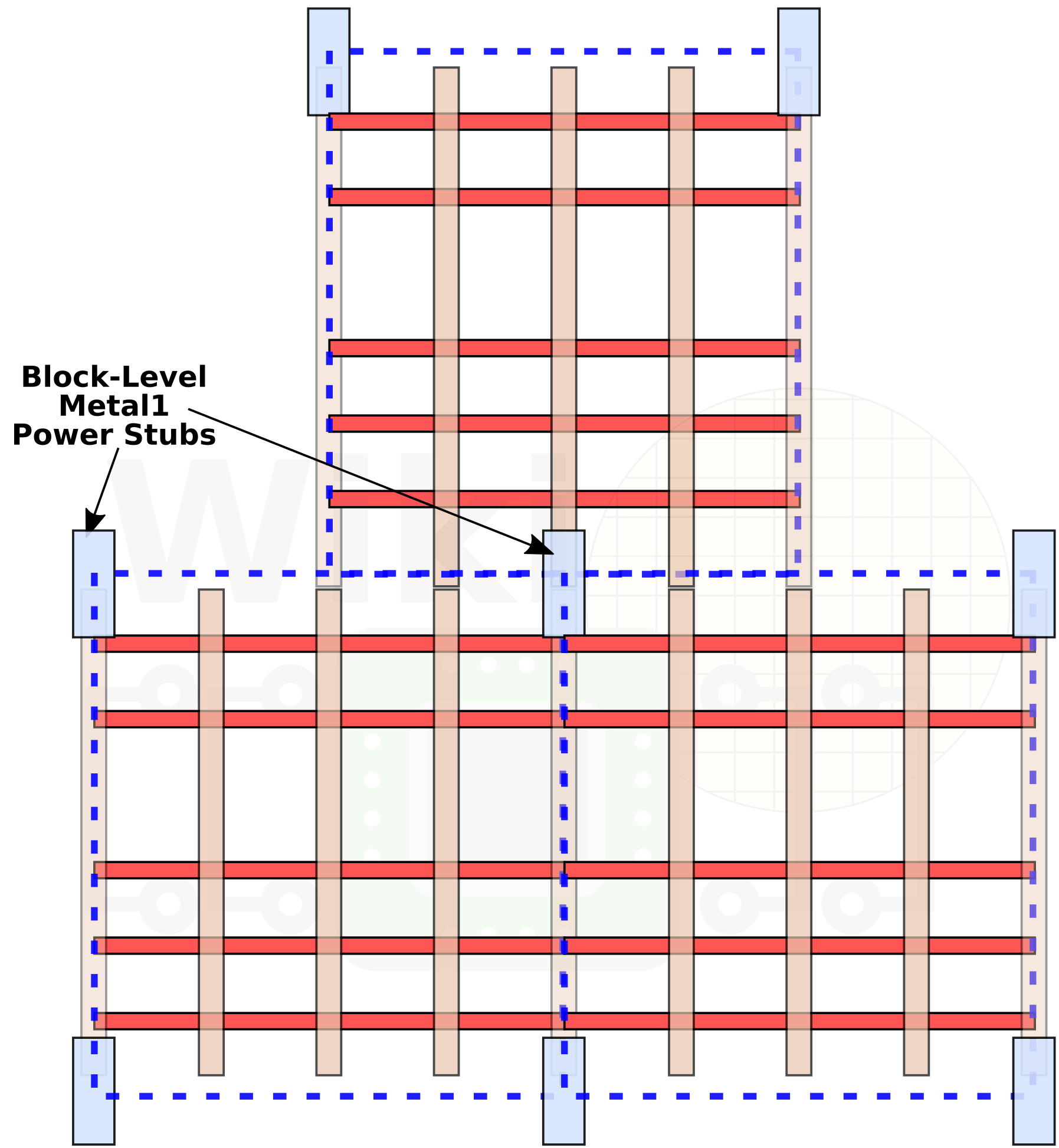
In order to realize the density advantages from the cell-level up the hierarchy to the block-level and ultimately the final product, a number of new technologies were created. One of these is a new feature they call a block-level power hook-up. Connecting the Metal 0 power rails to the Metal 2 power rails via the Metal 1 is usually done using Metal 1 stubs.
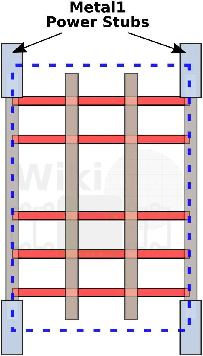
When joining multiple cells together, because those stubs are found inside the individual cells, a significant amount of the Metal 1 layer is used up by the power delivery itself.
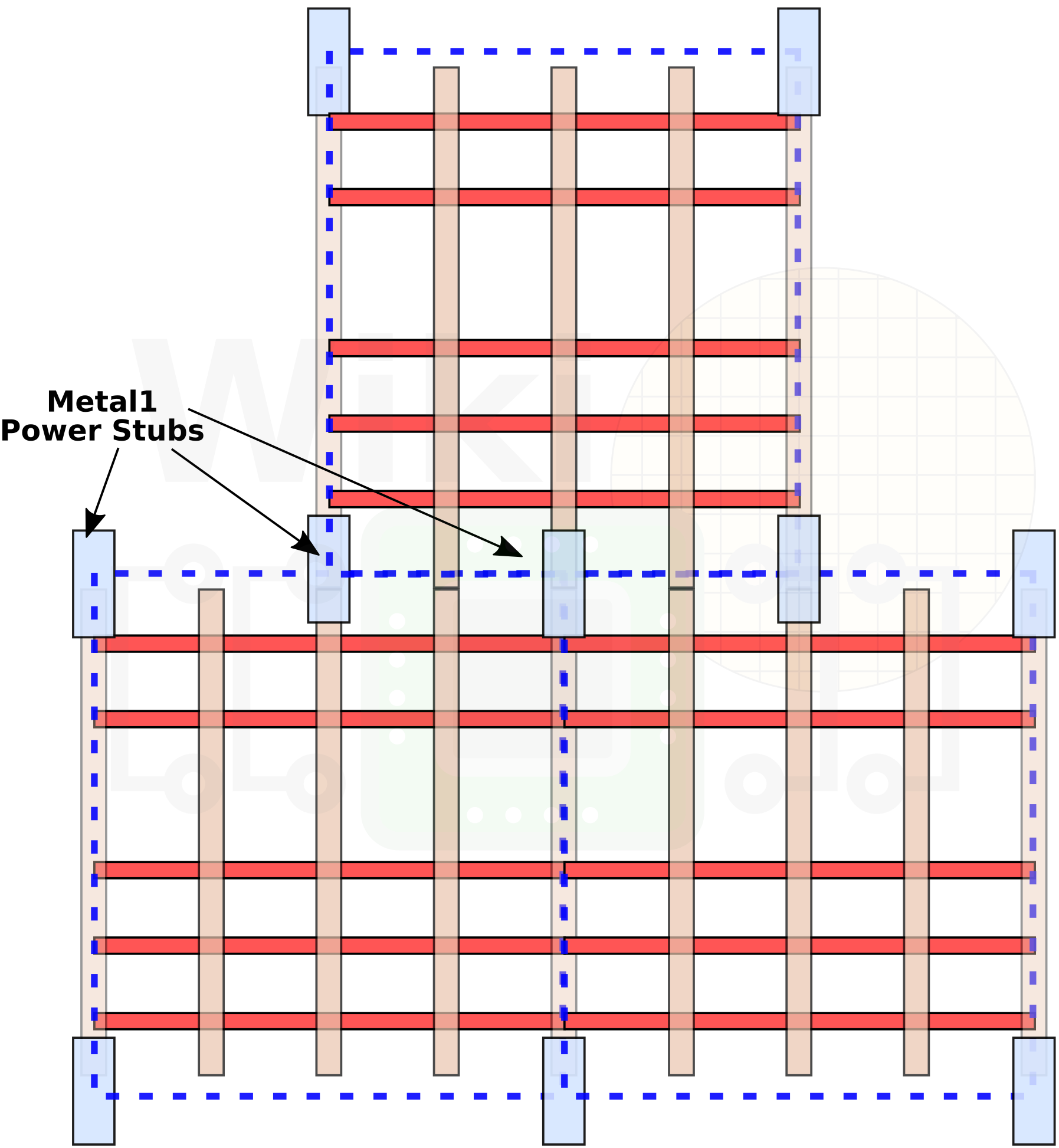
What Intel chose to do instead is to take those stubs out of the individual cells and instead apply them at the block level. There’s just one problem – it’s not a trivial change at all. In fact, it’s a really complex problem. By removing the power stubs from the individual cells, moving them to the block level requires greater awareness by the EDA tools. This isn’t something the tools can normally do. Intel says they have worked closely with EDA vendors on a power hookup solution that can be applied at the block level and that’s natively supported by the standard EDA APR tools. This solution allowed them to free up a significant portion of the Metal 1 layer which in turn further improved block-level density.
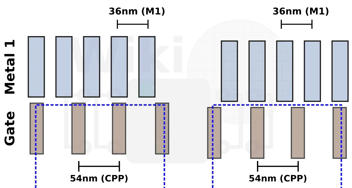
Metal 1 Misalignment Awareness
There is another problem involving the Metal 1 layer – misalignment. For Intel’s 10-nanometer, the gate pitch is 54 nm but the Metal 1 pitch is 36 nm. Those pitches were carefully chosen such that there is a 3:2 ratio between the two. In other words, for every 3 Metal 1 tracks, there are two poly tracks.
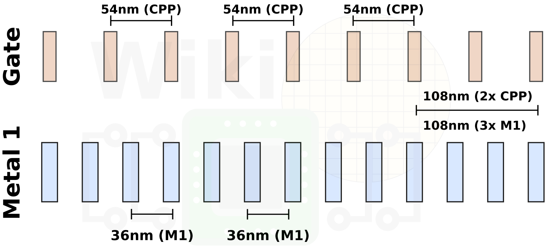
Due to the 3:2 ratio between the gate and M1, it’s possible to have a misalignment between the two depending on if the standard cell has an even number of poly tracks or odd. As with the power stubs issue, the alignment issue manifests itself at the block level. In those cases, the misalignment has to be honored and this becomes an EDA tool problem. Intel worked with EDA vendors to address this issue. To solve this, the placement tool has to understand the intimate alignment restrictions of their standard cell library and adjust the cell alignment so that both the gate and Metal 1 are aligned. To honor the misalignment, a gap must be left in the standard cell row.
A gap in the cell row means you have a reduction in area utilization. Instead of realizing the cell-level density improvements at the block-level, you are underutilizing the area. To solve this issue, Intel duplicated the entire standard cell library so that every cell includes two M1 variations. In other words, there is now an ‘aligned’ and a ‘misaligned’ version of every cell such that the placement tools are able to maximize the area instead of inserting gaps.
This feature required very close collaboration between Intel and the EDA vendors in order for the tools to become ‘alignment aware’ but it’s a necessary feature in order to realize the area benefits at the cell level also at the block level and ultimately at the full SoC level. At the synthesis and placement phases of development, a custom algorithm is used to check all the possible options and pick the optimal cell location/variant in the floorplan. Dr. Wang reported that from that co-optimization, depending on the type of block, they saw around 5-10% density improvement for blocks that already had high utilization.
At IEDM, Dr. Wang stated that both the ‘Power Hook-up Awareness’ and ‘Alignment Awareness’ have been natively implemented and optimized by EDA vendors and is supported seamlessly inside
the standard APR flows. These challenges are considered a solved problem.
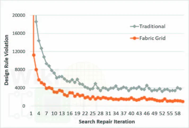
Global Fabric Grid
One of the new systems Intel developed for their 10-nanometer is a new grided logic fabric which is used for the tight-pitched layers at the block level. Given that the Metal 0, 1, and 2 are used in both the cell and at the block level, a new fan routing system was developed in order to ensure that resources are used efficiently and in such way that it eases place and routing afterward. A global routing grid has been predefined such that it’s correct by construction from a design violation stand point in terms of design and routing issues. From a design perspective, both the router and the standard cell pins honor the gridded system.
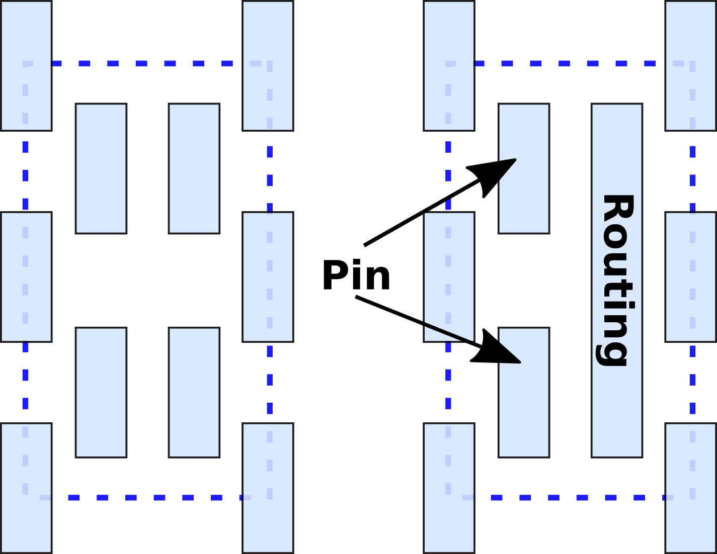
Dr. Wang reported that compared to traditional routing, the gridded logic can reduce the design rule repair runtime by 1.6x and it does so while achieving better design rule convergence.
Libraries Comparison
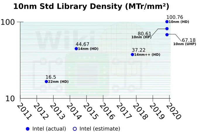
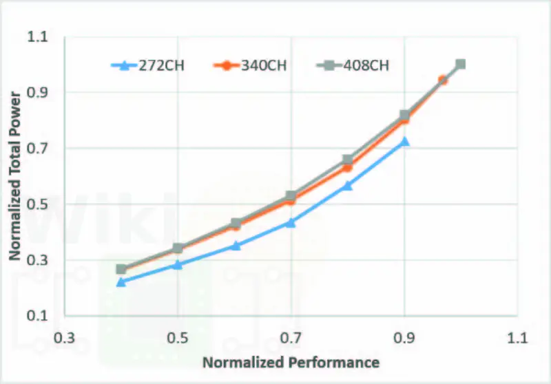
For their 10-nanometer process technology, Intel has three main standard libraries for logic – a high-density, a high performance, and ultra-high performance. They are 8-, 10-, and 12 diffusion lines high respectively.

At the cell density level, those cells are 0.8x and 0.67x as compact as the high-density cell. Intel’s 10 nm aggressive scaling means that even their ultra-high performance cells (the least-dense cells) are 1.8x the compaction of their own highest-density 14nm cells.
With more legs, the HP and UHP cells are capable of much higher performance due to the packing of more fins. The higher performance comes at the cost of higher capacitance. The graph below was reported by Intel for their three cells at ISO transistor-leg conditions for an unspecified industry standard Core IP design. In blue is the high-density cell which is geared toward lower power and as such is rather capped in terms of performance. It’s worth pointing out that the performance difference between the mid-height and tall cells isn’t very significant but it does incur 18% higher area penalty for this core IP. This implies that the tall cells are only really necessary for few specific products (e.g., client desktop parts).
–
Spotted an error? Help us fix it! Simply select the problematic text and press Ctrl+Enter to notify us.
–