
IEDM 2018: Intel’s 10nm Standard Cell Library and Power Delivery
3 Main Library Offerings
Through considerable analysis, Intel arrived at three main logic library offerings – a high-density cell, a high-performance cell, and an ultra-high performance cell. All three libraries are 6T libraries, each with a custom-designed BEOL.
- Short Library – HD Cells – cells can accommodate 2 fins per cell height, 2p+[2+1]n
- Mid-Height Library – HP Cells – cells can accommodate 3 fins per cell height, 3p+[3+1]n
- Tall Library – UHP Cells – cells can accommodate 4 fins per cell height, 4p+[4+1]n
Short Cells
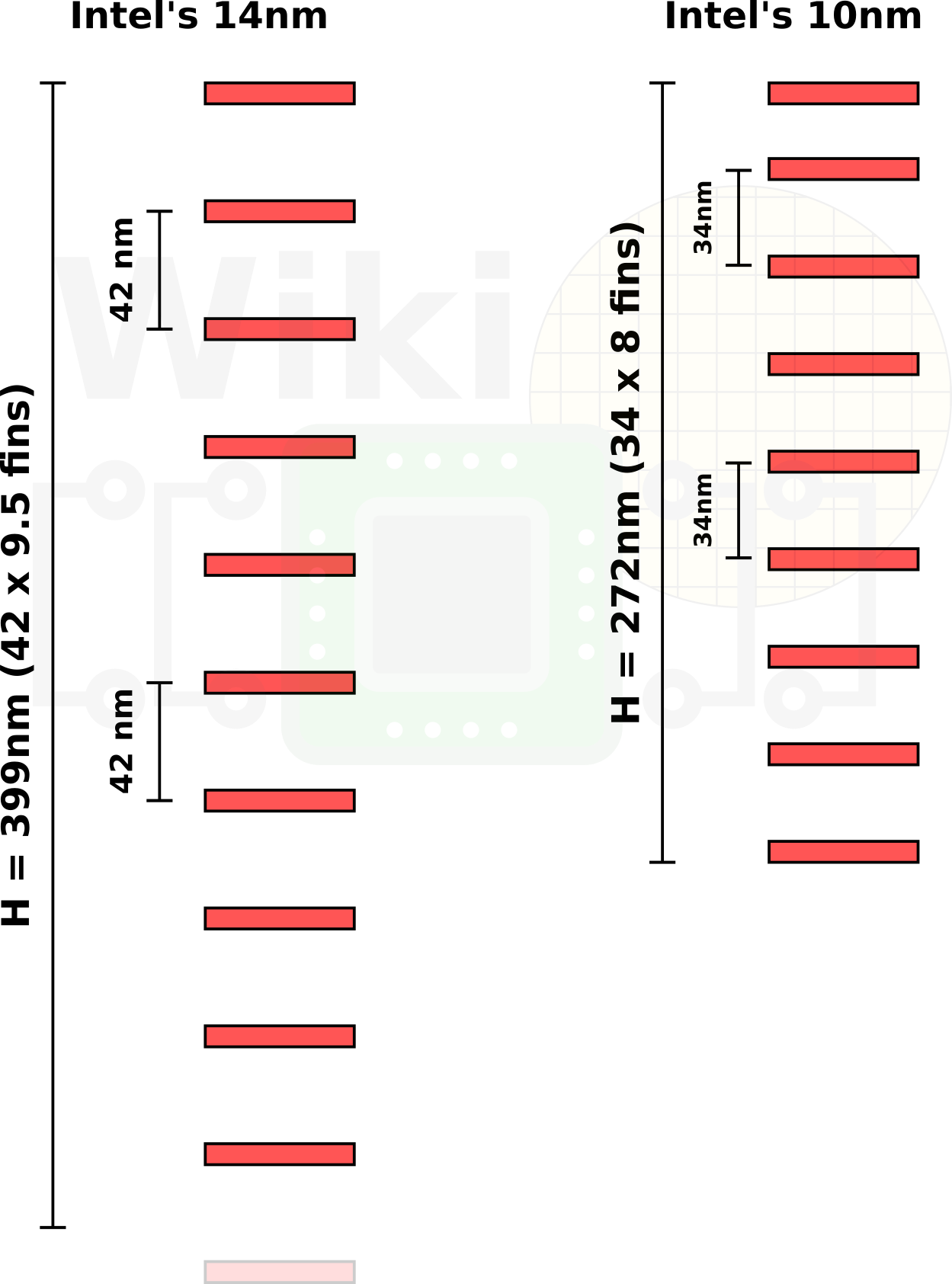
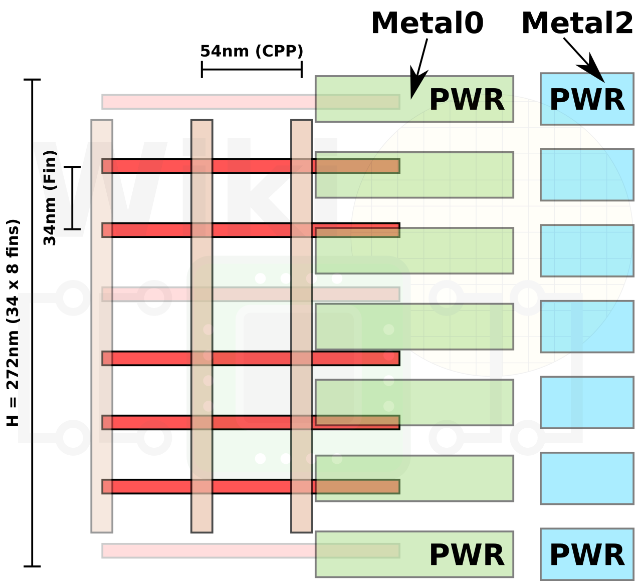
Short cells favor lower power and high density over absolute performance. These cells are optimized for minimum capacitance and area at lower drive currents. Due to its density advantage, this library is also ideal for cost-sensitive applications. Dr. Wang stated that applications for this library include graphics, uncore, SoC, and FPGA products. Readers who follow our articles closely may already be familiar with this cell from our June article. Those cells can accommodate 2 fins per leg. In other words, they have 2 P-fins per transistor and 2 N-fins per transistor with an additional option for another N-fin for various logic functions that find the extra active fin useful in situations where there is a continuous poly line. The third fin can be used for various prioritizations (e.g., NAND over NOR). The cell has a height of eight diffusion lines (FP=34nm) or 272 nanometers.

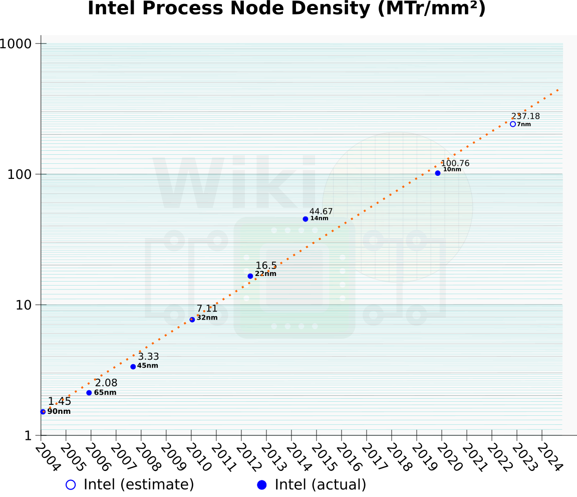
This is Intel’s highest density cell to date. A full chip filled with just those cells can pack, based on the MTr/mm² metric, around 100.76 million transistors per squared millimeter. This is a 2.7x compaction value versus their highest-density cell on their current 14-nanometer process. The 14 nm HD cell was 9.5 diffusion lines heigh at 399 nm.
Despite being incredibly late, the fact that both the 14-nanometer and 10-nanometer nodes have made much larger than 2x density jumps, the overall trend is only a minor hiccup for Moore’s Law. We would have to wait for 7-nanometer to see if anything major changes.
The high-density cell power delivery scheme includes two levels of power rails at the cell border. There are two power rails at the cell border on the Metal 0 layer which runs parallel to the fins and two more power rails at the cell border on the Metal 2 layer. This leaves each cell with five dedicated signal metal tracks for efficient intra-cell connections. Because the main optimization point here is density, both the Metal 0 and Metal 2 rails are intended to be shared between two adjacent standard cell rows.
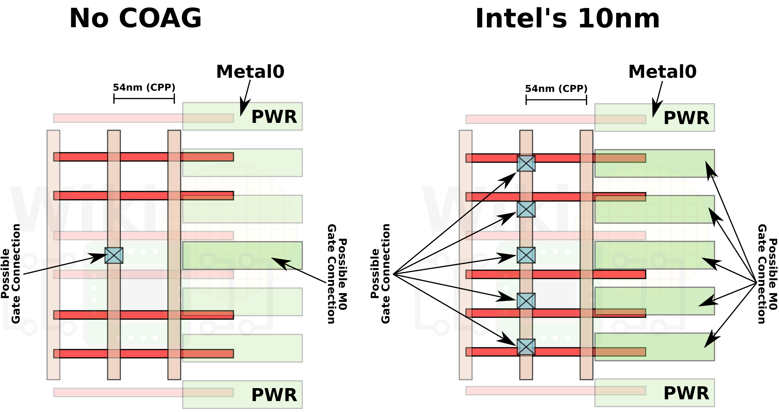
One of the new technologies that Intel introduced with their 10-nanometer node is the contact over active gate (COAG).
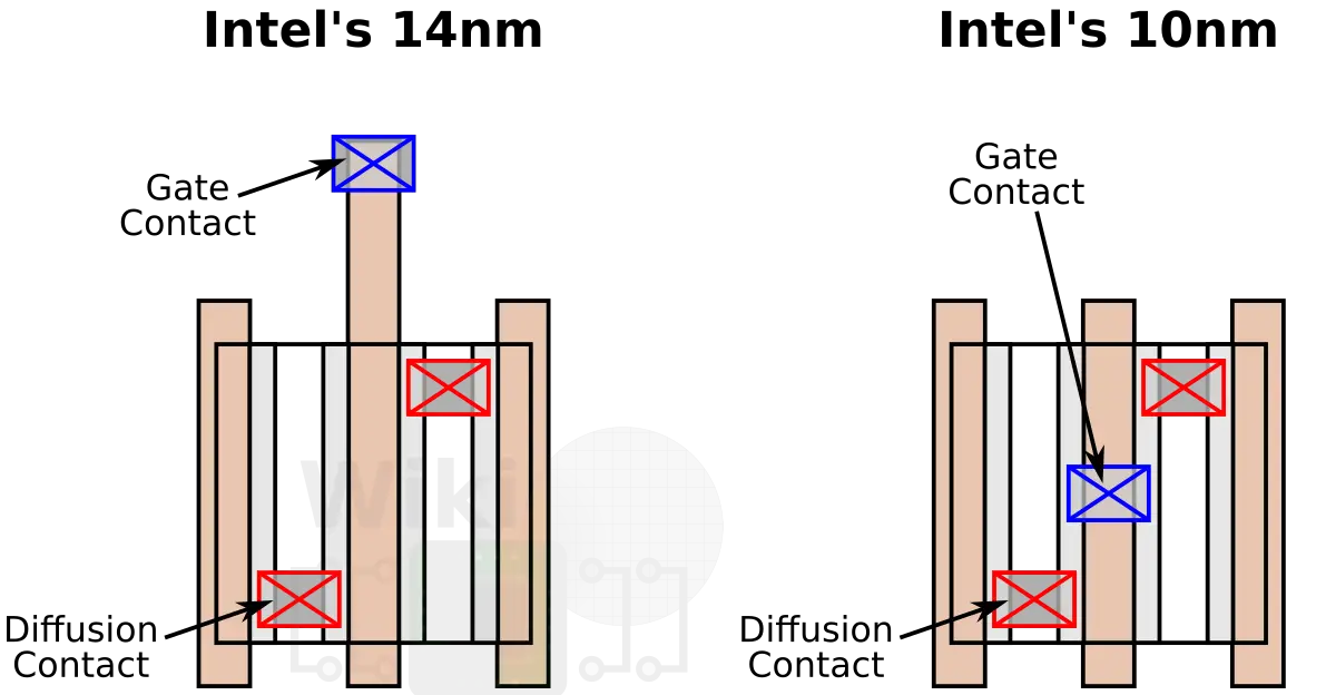
The benefits of COAG are immediately apparent when looking at the high-density cell design. Without COAG, the gate contact has to be dropped off the active region and over the isolation region. To do this, the dead space between the two types of active fins has to be larger. This means that the cell itself has to be slightly taller and you lose the ability to add another fin for additional optimization capabilities. By contrast, Samsung is also introducing COAG around their 4-nanometer node but they are doing so purely for density reasons.
One of the other important benefits of COAG is the ability to shift the contact up and down as desired. They leverage this feature extensively with all their standard cells. For example, the HD cell can now connect with the gate at every one of the five signal tracks.
–
Spotted an error? Help us fix it! Simply select the problematic text and press Ctrl+Enter to notify us.
–