
ISSCC 2018: The IBM z14 Microprocessor And System Control Design
Central Processor (CP) Chip
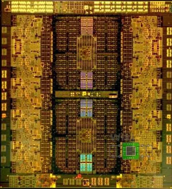
The z14 microprocessor or central processor (CP) chip integrates 6.1 billion transistors on a 696 mm² die. Utilizing 17 metal layers with 23.2 kilometers of signal wires, the chip has roughly 20,000 C4 solder bumps. z14 designed to operate at a clock frequency of 5.2 GHz.
[foogallery id=”1268″]
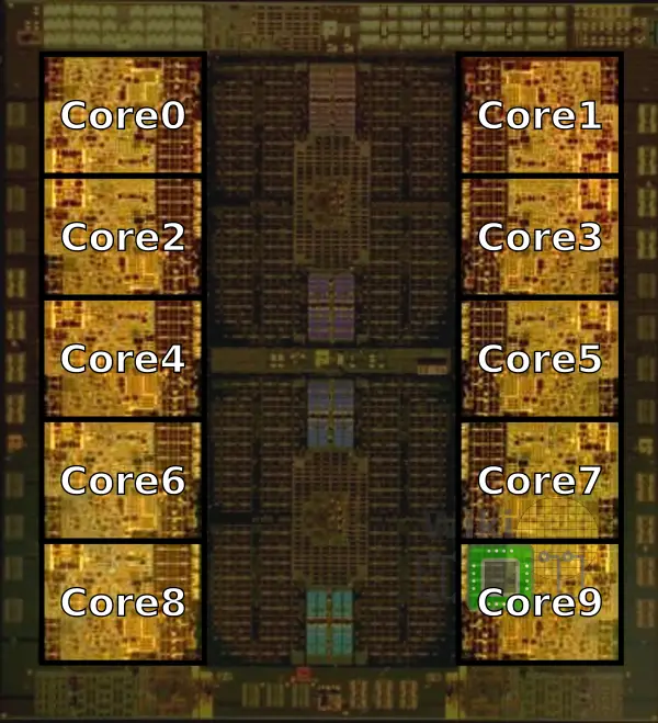
The die itself incorporates 10 cores arranged in two columns with the level three caches in the center. The z14 cores are very large, measuring 28 mm² in die area. It’s worth noting that each core also incorporates the z14 analytics and compression engines. As far as caches go, each core has 256 KiB of L1 cache split evenly between the instruction and data caches and 6 MiB of L2 cache with 2 MiB dedicated for the instruction cache and 4 MiB allocated to the data cache. The L1 cache is designed using SRAM cells while the L2 caches utilize the high-density eDRAM cells.
Located between the two columns of cores is the shared L3 cache. The cache is broken down into two clusters at the top and the bottom of the die. The clusters were designed very similarly to the L4 cache found in the SC chip with 16 MiB of eDRAM slices surrounding the control and directory in the center. With two clusters of 64 MiB each, the z14 has a total of 128 MiB of L3 eDRAM cache. It’s worth noting that IBM added symbol based Reed-Solomon ECC to their L3 cache with the z14 in order to improve data integrity. This replaced the prior bit-based single error-correction double-error detection (SEC/DED) technique which was used in the z13. In theory, up to one out of every eighteen eDRAM macros can fail and the system will still be up and running.

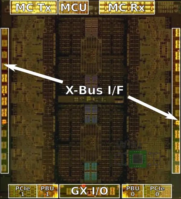
To the left and right sides of the die are three X-bus links which fully interconnect all the CP chips within a cluster in a drawer. Those are single-ended 5.2 Gb/s per lane for a link bandwidth of 800 Gb/s and a total chip bandwidth of 2.4 Tb/s. The memory interface and controller sit at the top of the die. The memory interface is 9.6 Gb/s per lane for a total of 1.6 Tb/s of main memory bandwidth. At the bottom of the die is the PCIe and PCIe controller (PBU) as well as the GX infiniband interface. Those interfaces have a total bandwidth of 700 Gb/s.
Design Efficiency Or Efficient Designer
When working on large designs, it’s often advantageous to rely on a system of hierarchies in order to streamline the design. A hierarchy allows engineers to reuse blocks, deal with more manageable pieces of logic, and allow tools to run faster on smaller blocks. Unfortunately, the hierarchy creates artificial boundaries in the design that cannot be eliminated afterward. Ultimately, this restricts optimizations to smaller blocks, making large-scale (i.e. inter-block) optimization very difficult.
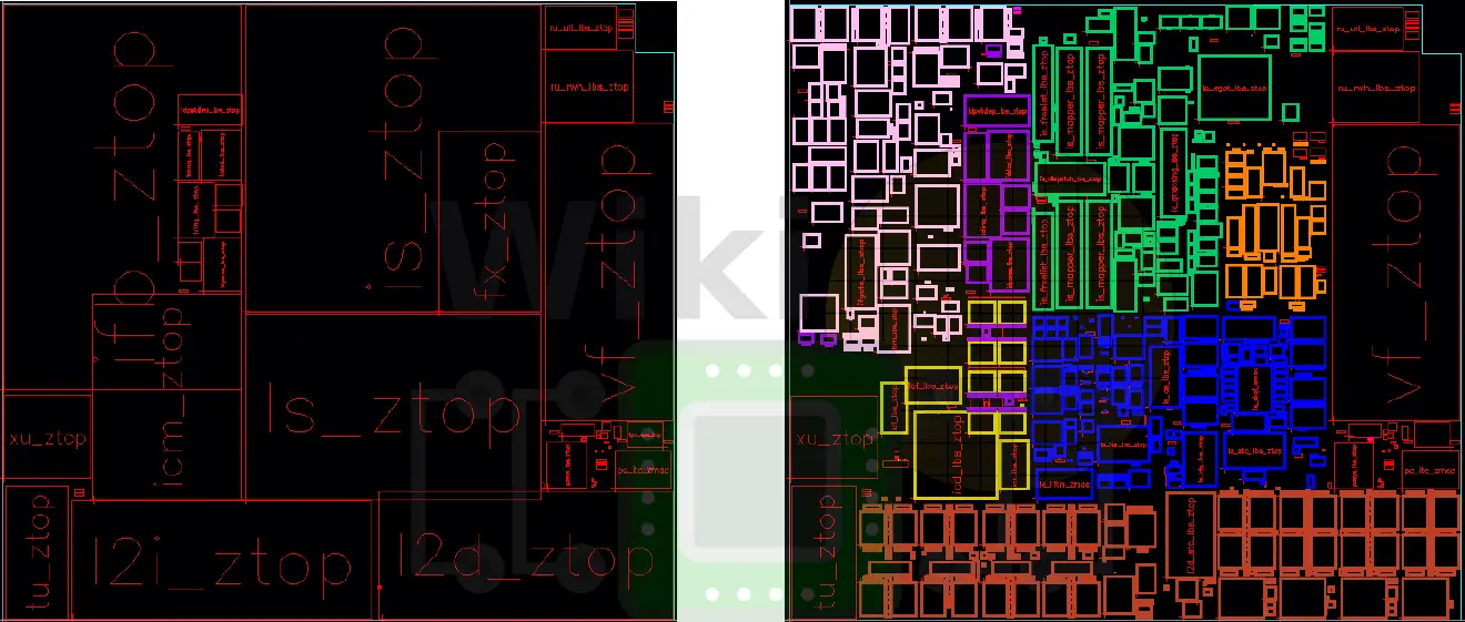
The z13 floorplan is shown below. The large blocks that make up the core are very regular with straight borders. The image on the right shows the small individual synthesized blocks inside of unit hierarchy. What can be observed is that the unit hierarchy is preventing optimizations across unit boundaries. For example, the unit in blue is packed very tightly while the unit in pink is underutilizing its area. In both places, the hierarchy is creating artificial boundaries across which no optimizations are taking place.
With the z14, IBM tried to reduce levels of hierarchy in order to optimize across larger areas of the die in order to improve the overall efficiency. By eliminating some of that hierarchy, IBM was able to optimize across the entire floorplan, and further optimizing the placement and routing across the entire core. The z14 floorplan shown below improved area utilization by 30%, reducing whitespace and optimizing across unit boundaries. Shown below, the floorplan of the z14 now utilizes the area much more efficiently with units being more compact in irregular regions. This also allowed them to fill holes and move blocks to areas that would normally be in one unit to another area. It’s worth pointing out that since the core itself is another level of the hierarchy, the blocks within the core are restricted to the rectangular boundaries of the core which still results in various inefficiencies.

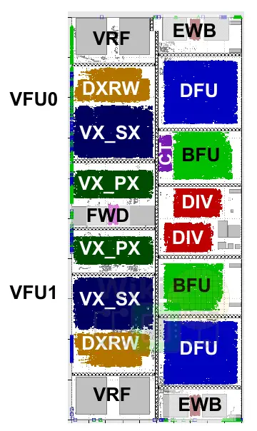
Historically, IBM used to do a lot of custom designs and relatively small synthesizable blocks. Those would, in turn, be combined into larger units. Starting with the z13, IBM developed a new methodology called large blocks synthesis which allowed them to synthesize large portions of the design. In the z13, the largest synthesizable blocks could be as large as 4 mm². Being their first design to use this methodology, the z13 had some large area inefficiencies. Below is a picture of the z13 vector floating unit (VFU). Making up an area of 3.9 mm², it can be seen that there is a large amount of unutilized area in the whitespace.
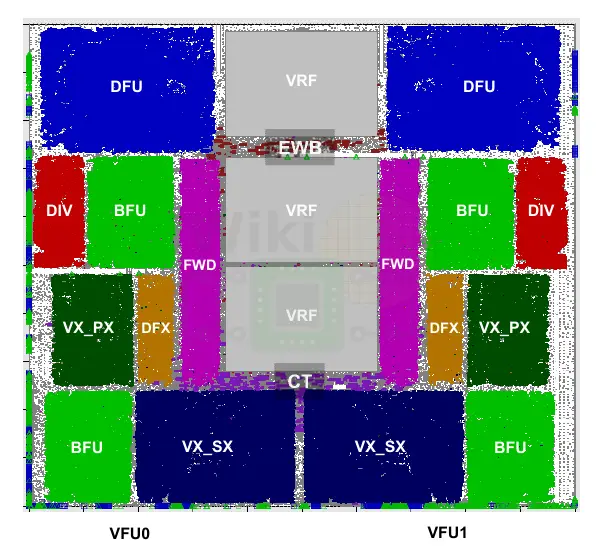
In the z14, they decided to go after those inefficiencies. Below is the z14 VFU which now takes up 1.3 mm² of an area (1.4 million gates) for roughly 3x shrink. Note that this includes the addition of two new large binary float units (BFUs). The z14 unit has 31% higher area utilization which can be seen from the reduction in white regions.
–
Spotted an error? Help us fix it! Simply select the problematic text and press Ctrl+Enter to notify us.
–