ISSCC 2018: AMD’s Zeppelin; Multi-chip routing and packaging
SerDes
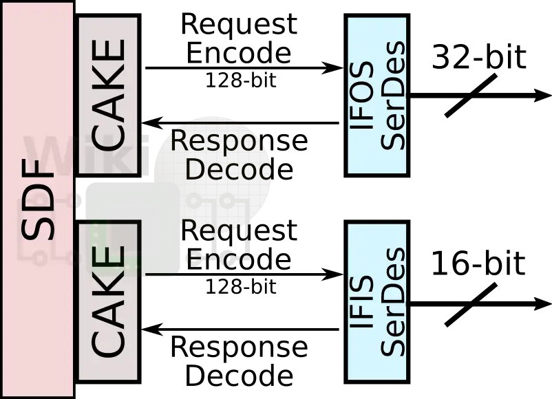
Interfacing between the Infinity Scalable Data Fabric and the SerDes is the CAKE which takes requests and encodes them into 128-bit packets to be sent over any SerDes. Responses are also decoded by the CAKE back to the SDF. As with everything else that is attached to the SDF, the CAKEs operate at DRAM’s MEMCLK frequency in order to eliminate clock-domain crossing latency. Due to the performance sensitivity of the on-package links, the IFOP links are over-provisioned by about a factor of two relative to DDR4 channel bandwidth for mixed read/write traffic. The IFOP SerDes do four transfers per CAKE clock while the IFIS SerDes do eight.
IF InterSocket SerDes
Since the IFIS links double up as PCIe and SATA protocols, some more restrictions apply. They operate on TX/RX 16 differential data lanes at roughly 11 pJ/b (by the way, those links are aligned with the package pinout of standard PCIe lanes). Because they are 16-bit wide they run at 8 transfers per CAKE clock. CRC is transmitted along with every cycle of data Compared to the IFOP, the IFIS links have 8/9 of the bandwidth due to the 16b data and in-band CRC overhead.
IF On-Package SerDes
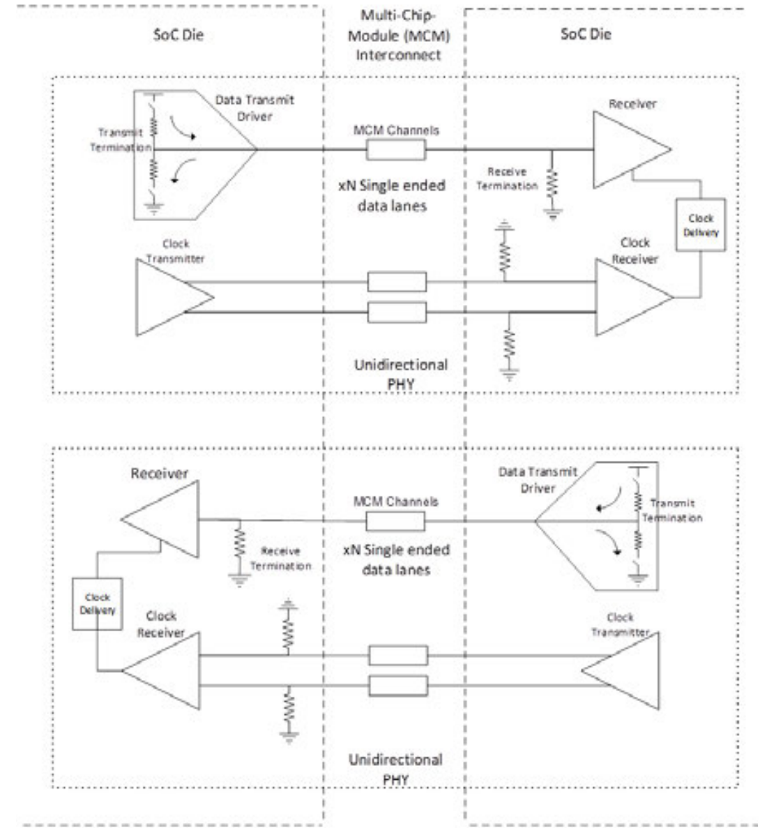
For their in-package SerDes, AMD designed a fairly straightforward custom SerDes suitable for short-in package trace lengths which can achieve a power efficiency of roughly 2 pJ/b. This was done by using a 32-bit low-swing single-ended data transmission with differential clocking which consumed roughly half the power of an equivalent differential drive. They utilize a zero-power driver state from the TX/RX impedance termination to ground while the driver pull-up is disabled. This allows transmitting zeros with less power than transmitting ones which of course was also leveraged for when the link was idle. Additionally, inversion encoding was also used in order to save another 10% average power per bit.
Bandwidth
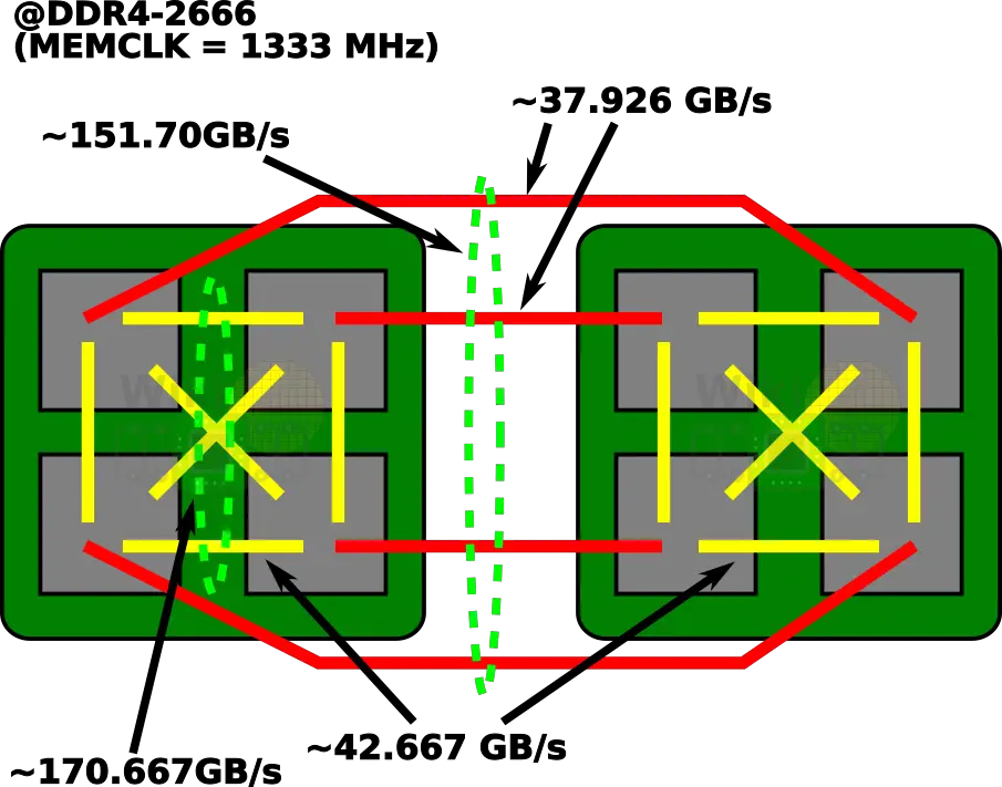
Currently, the highest officially supported DDR4 rates for AMD’s first generation Threadripper and EPYC is DDR4-2666 or a MEMCLK of 1333.33 MHz. For EPYC this means die-to-die links have a bandwidth of roughly 42.667 GB/s for a bisectional bandwidth of 170.667 GB/s. Socket-to-socket links have 8/9 the bandwidth at 37.926 GB/s for a bisectional bandwidth of 151.70 GB/s. Faster, overclocked memory, will yield higher bandwidth.
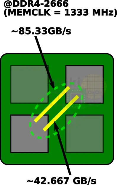
For the Ryzen Threadripper, the die-to-die links are doubled with two IFOP SerDes meaning the bandwidth is roughly 85.33 GB/s.
Cost Analysis
Although AMD presented multi-chip vs monolithic chips comparisons before, at ISSCC we got to hear some more specific numbers. With each Zeppelin being 213 mm², a 4-die multi-chip unit is 852 mm². AMD estimated that a single-chip design with 32 Zen cores would be roughly 777 mm². This is taking into account the reduced area size due to the elimination of components such as some of the CAKEs and the IFOP SerDes. In addition to preventing AMD from reusing the die for the desktop market segment, they estimated that the manufacturing and testing cost for the larger die would be roughly 40% higher. When looking at only a 32-core product, AMD estimated that the yield would be roughly 17% lower than their current 4-die chip. As part of this lower yield, they also estimated that cost for a full 32-core product to be roughly 70% higher than their 4-die chip.
It’s important to note that those numbers were for a full 32-core product only. We estimated that Intel’s Skylake XCC die is around or less than 700 mm², meaning their yield should be better than AMD’s estimates. Additionally lower core count parts are offered in order to substantially reduce this cost. In fact, their XCC die spans all the way from their 28-core models to a quad-core.
Scaling Using Different Solutions
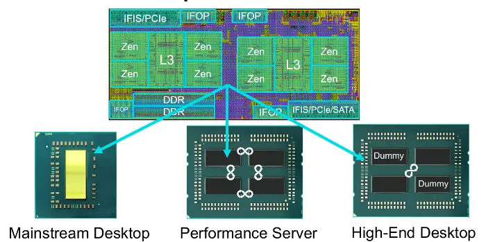
With the design of the Zen core well underway, they needed a solution that would scale from mainstream desktops to server processors. AMD achieved that goal through the ground-up development of the Zeppelin SoC module that could scale from a single die to a four-die multi-chip module. This allowed them to develop three distinct processor families, addressing each of market segments they were after.
At this year’s conference, both Intel and AMD presented their approaches to scaling the number of cores across a range of products. Intel developed a mesh interconnect architecture, enabling a modular design to scale well beyond what their ring interconnect was able to offer. AMD has gone with a chiplet approach instead. Both approaches have their own advantages and disadvantages. While there is much debate as to which solution is a “better solution”, the reality is that both companies have gone with the solution that best addresses their needs, their resources, and their manufacturing capabilities.
Derived WikiChip Articles: Infinity Fabric, Zeppelin, Zen Microarchitecture
–
Spotted an error? Help us fix it! Simply select the problematic text and press Ctrl+Enter to notify us.
–
