Samsung 5 nm and 4 nm Update
Samsung’s slower ramp of 7-nanometer is tightly coupled to EUV readiness. Over the past year, we have seen throughputs slowly improving to acceptable levels. Currently deployed NXE:3400B systems are operating at 250 W or higher. This, along with several other improvements such as uptime as meant that EUV is now ready for high volume manufacturing.
With Samsung finally getting its 7-nanometer process out the door with the Exynos 9825, it’s time to look at next-generation process node.
Roadmap
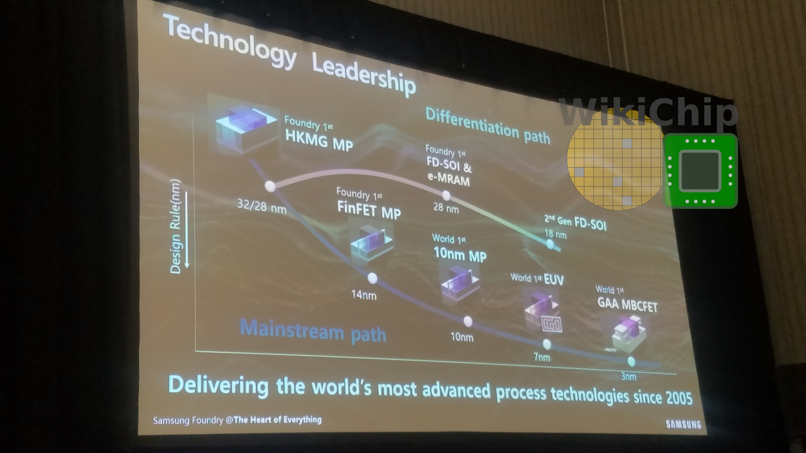
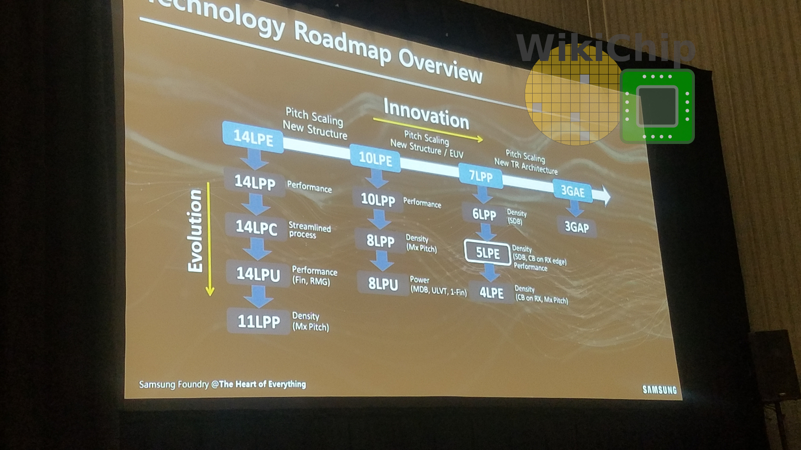
The roadmap is very similar to what we reported on it last year, however, there is a number of interesting changes. At a high level, Samsung is sticking to the strategy they outlined a few years ago – produce four major nodes and derive smaller and highly incremental follow-up nodes with various PPA enhancements. To that end, Samsung is currently at its 7LPP point. The first modification in the roadmap is the insertion of a new 6-nanometer node. Samsung inserted the 6 nm earlier this year on the same week TSMC announced its 6 nm node. Samsung 6LPP simply introduces SDB thereby providing them with a 1.18x density improvement. Another change is the removal of the 4LPP node, leaving just 4LPE on the roadmap which we will discuss in a bit more detail later on. Lastly, Samsung renamed 3GAAE and 3GAAP to 3GAE and 3GAP.
Samsung roadmap is the least risky roadmap of the last three leading-edge companies. Every one of the evolutionary nodes is highly incremental, often introducing just a single change. This allows them to mitigate the risk of new nodes by stripping away some of the scaling boosters they introduced earlier and adding them back on at a follow-up node once yield learning matures. The downside of this is that Samsung’s major nodes are fairly spaced out and in between major nodes they fall behind TSMC in PPA.
5LPE
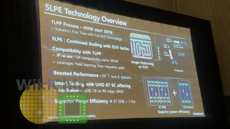
At a high level, the 5LPE node is really an extension of the company 7-nanometer process and is planned as a 2nd generation EUV process, building on the learning from 7LPP. To that end, 5LPE uses the same 7LPP transistors, SRAM and offers GR compatibility.
5LPE, however, does introduce a number of new enhancements. The largest enhancement is the new 6T UHD library that comes with SDB and a 36 nm M2 as well as CB on the edges of the active region pattern (RXN/RXP). For ultra-low power / always-on transistors, Samsung also added single-fin devices.
PPA
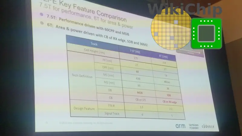
5LPE offers a number of benefits over 7LPP, depending on the migration path chosen. Through transistor improvement enhancements, Samsung is claiming up to 11% performance improvement over its 7LPP process when using the 5LPE 7.5T library. Alternatively, moving to the 6T library will allow for 0.70x density improvement.
| 5LPE | ||
|---|---|---|
| 7.5T (HD) | 6T (UHD) | |
| FP | 27 nm | |
| CPP | 60 nm | 54 nm |
| M1 | 40 nm (Bi) | 40 nm (Uni) |
| M2 | 60 nm | 36 nm |
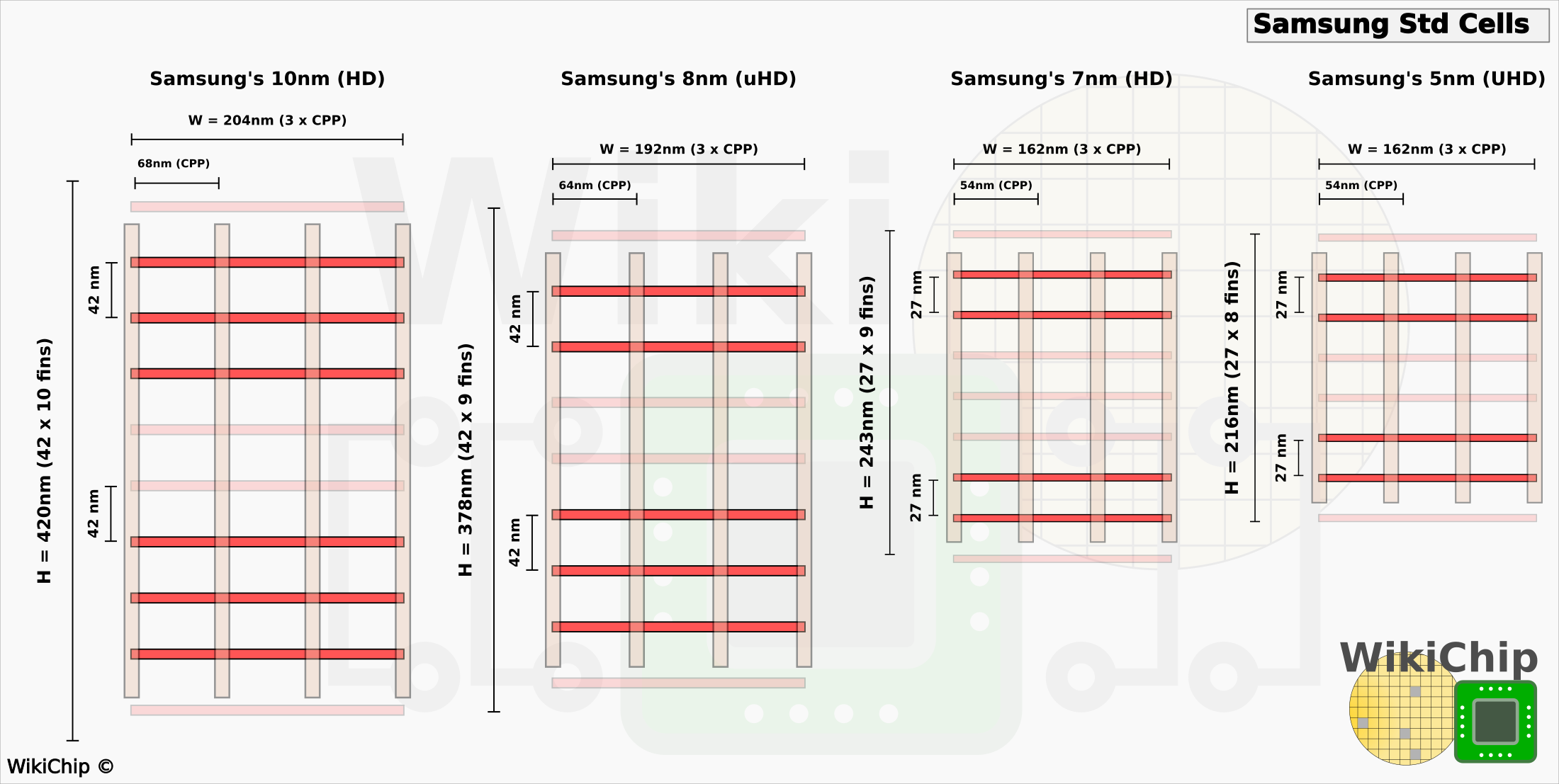
The difference between the two libraries is quite minor and features identical transistors as 7LPP – same FP, same PP, buts lightly improved profile. The HD library is a 3p+3n along with a 60 nm poly pitch and a MDB. The UHD is a 2p+2n with SDB and uses the 54 nm tighter poly pitch.
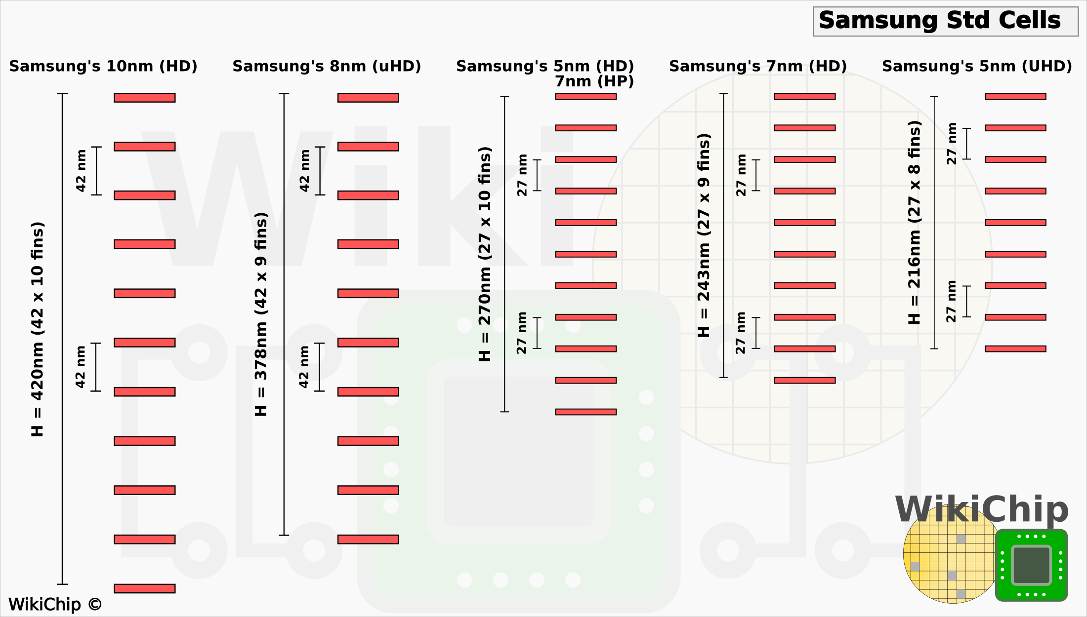
A better way to understand Samsung’s standard cell library evolution is through a performance/active diff lines/cell comparison. The current trend is 10 diffusion lines on 7 HP, down to 9 diffusion lines 7 HD, and finally down to 8 diffusion on 5 UHD. Compared to its 10-nanometer, Samsung’s 7LPP has a higher drive current per fin, therefore starting out with the same number of diffusion lines per cell gives you higher performance. Along with the shrink, you have better PPA per cell. Both 8-nanometer and 7nm high-density cells remove a single fin, giving you better area at similar performance to the prior node. The new 5 nm UHD cells continue this trend further by removing another fin, which, when combined with the slightly enhanced transistors, provides a slightly better power-area improvement (but not performance) – at least in theory, at a very high level.
The new ultra-high density (UHD) 6T library replaces the previously 7LPP HD library which had nine diffusion lines. The new UHD library removes another diffusion line, yielding a cell height of 216 nanometers. What’s also new here is the introduction of CB on the active RXN/RXP edge.
Samsung also added single-fin low-leakage devices which are reported to provide up to 20% lower power.
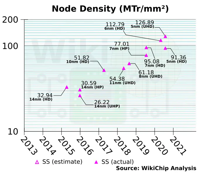
By our estimates, Samsung 5 nm node UHD cells has reached close to 130 MTr/mm² which is the first Samsung node to exceed both Intel’s 10-nanometer node and TSMC 7-nanometer nodes in terms of density. It’s worth adding that early next year, TSMC will ramp its N5 node which is considerably denser than anything Samsung is offering. Given the timing we also expect TSMC to ramp N5 before Samsung ramps 5LPE.
4LPE
Samsung’s last FinFET node will be the 4LPE node. 4LPE is similar to 5LPE but shrinks the M1 pitch from 40 nm to 28 nm and the M3 from 36 nm to 32 nm. We have also heard that the fin pitch is planned to be reduced to 25 nm but we could not formally confirm it. With the few numbers we currently have, we have estimated 4LPE to have a cell-level transistor density of 137 MTr/mm². Planned for around 2021, this will be the least dense process compared to both TSMC N5 and Intel’s 7 nm nodes.
–
Spotted an error? Help us fix it! Simply select the problematic text and press Ctrl+Enter to notify us.
–

