
VLSI 2018: GlobalFoundries 12nm Leading-Performance, 12LP
Reducing the Resistance
GlobalFoundries spent most of their effort addressing the transistor resistance (RON).

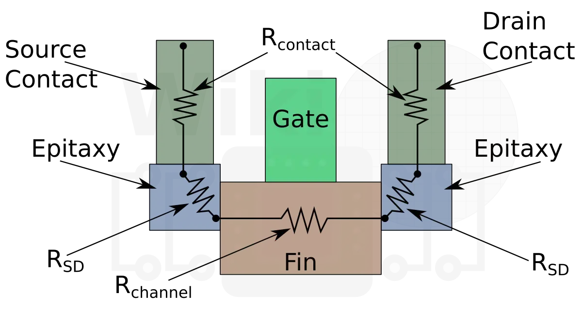
From a cross-sectional view, the path of the RON is shown below. The three major components addressed were the channel resistance (Rchannel), the source-drain resistance (RSD), and the contact resistance (Rcontact).
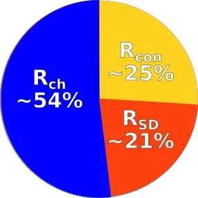
Although they did not give an exact breakdown, a graph of the breakdown was shown at the presentation. We have reproduced the graph below and extrapolated the percent breakdown (might be slightly off). The channel resistance is around 54%, the contact resistance is around 25%, and the source-drain resistance in the epitaxy region is around 21%.
Contact Resistance
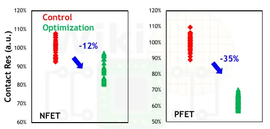
To further enhance the contact resistance, GlobalFoundries optimized the contact profile by enlarging the bottom contact size, increasing the overall contact area. The doping profile directly under the tranch contact was also optimized in order to reduce the height of the contact barrier and reduce the contact resistance. The two optimizations were reported to provide around 12% reduction in contact resistance for nFET and around 35% reduction for pFET.
Source-Drain Resistance
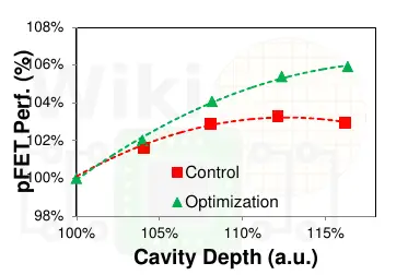
To further improve the pFET performance, GF modestly reduced the PLE (pattern loading effect) by optimizing the embedded silicon germanium cavity profile. The cavity in 12nm is now slightly deeper in order to allow for more eSiGe, improving channel strain. The 12nm 40-fin device showed around 4% improvement while the SDB devices showed around 5% improvement (2-fin devices saw no improvements).
For the nFET transistors, the active phosphorus dopant density was increased through the optimization of the Si-P epitaxial process which is said to deliver around 6% nFET improvement in the Ron resistance over the comparable control conditions.
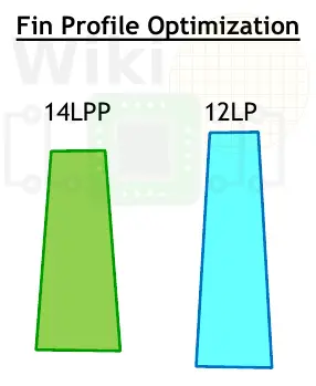
Channel Resistance
–
Spotted an error? Help us fix it! Simply select the problematic text and press Ctrl+Enter to notify us.
–