
OCP Makes a Push for an Open Chiplet Marketplace
Two major trends have been defining the future of silicon in the data center and edge for the coming decade. Specialized devices are becoming key to workload-intensive applications. In addition to GPUs and FPGAs, new types of programmable accelerators are emerging for networking and artificial intelligence. Some companies are also integrating those accelerators on-chip while others are offering them as separate attachments. Along with specialization, the industry started seeing the trend of de-integration. The increased cost of silicon has changed the economics of continuous integration, resulting in the rise of chiplet architectures, driving the need to split circuits into separately partitioned components that could be manufactured with different processes – sometimes by different companies.
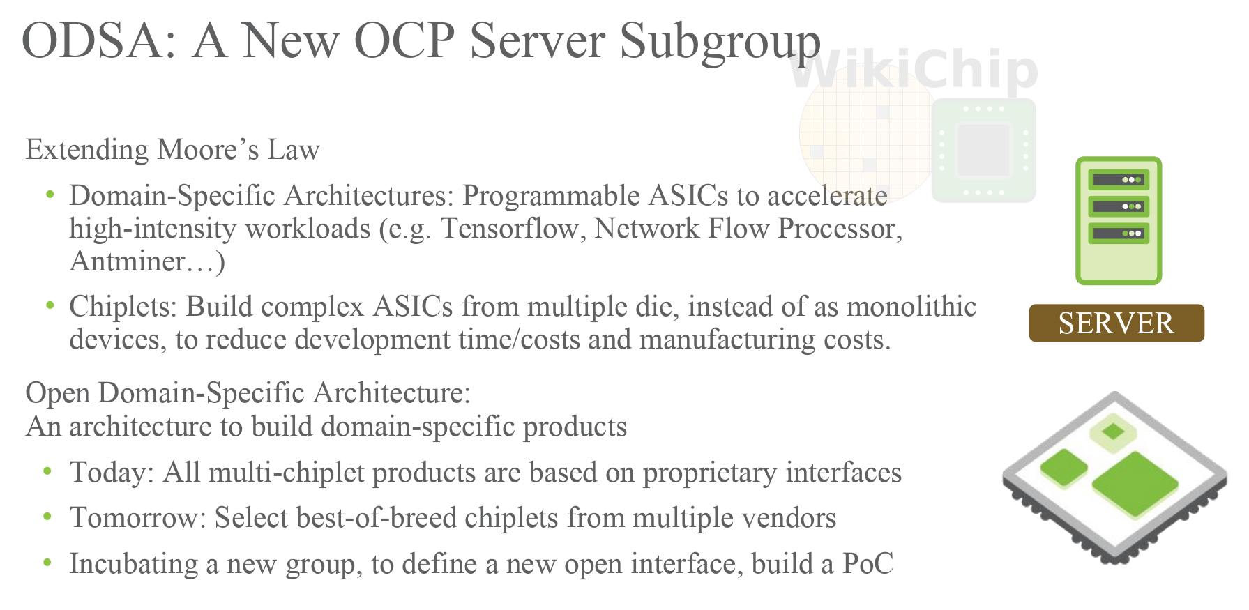
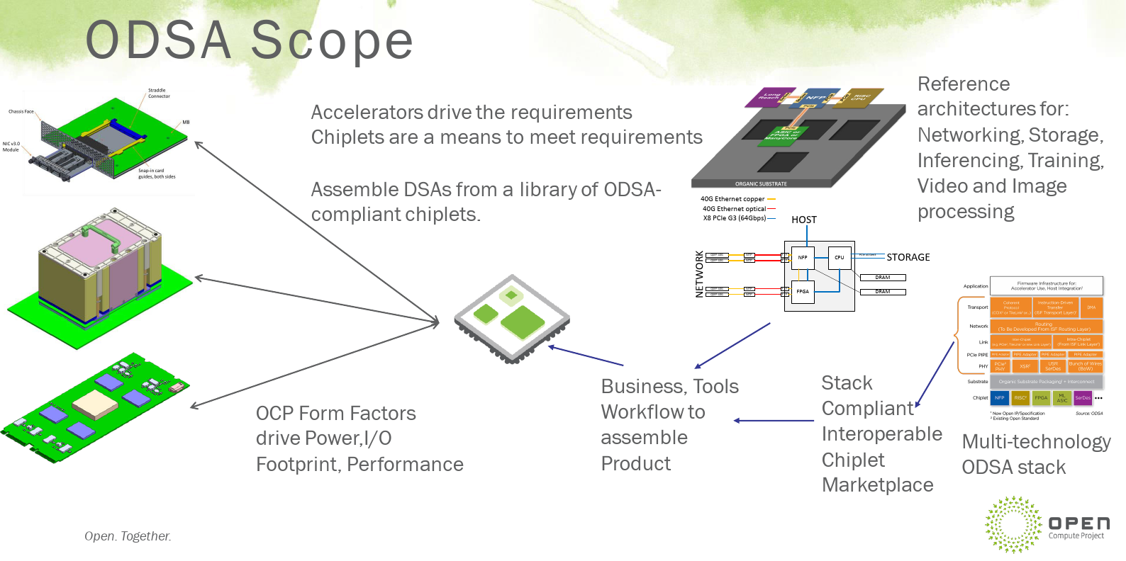
In late 2018, the Open Compute Project (OCP) started a new subgroup called the Open Domain-Specific Architecture (ODSA). Their primary market focus is the data center and the edge market. In fact, they are a subgroup of the OCP Server Work Group. Their active effort is situated strategically at the intersection of the two major trends – specialization and disintegration. Bapi Vinnakota, OCP ODSA Workgroup Lead at Netronome, told WikiChip “Many members of the ODSA group foresaw some of the trends we are currently seeing and we wanted an industry-wide collaboration to help.â€
The use of de-integration and chiplets is not a new concept. Many of the major semiconductor companies have been shipping such products for a few years now. Huawei Kunpeng (Taishan v110), AMD Rome (Zen 2), and Intel’s Stratix 10 FPGAs all make extensive use of chiplets. Current architectures take advantage of this to create custom SKUs, shorten development time and reduce development cost, and improve yield.
There are inherent limitations to those lone-wolf designs. The current approach means they are left with a narrow selection of chips. For example, both AMD and Huawei have their own I/O die and a compute chiplet which allows them to scale up the cores but not much else. While not impossible, neither company can add additional functionality such as an FPGA or other accelerators from a third party without additional work by everyone involved – and this currently requires adopting a proprietary solution (e.g., Infinity Fabric from AMD). Intel has been working on a solution to this problem. In collaboration with DARPA, the company introduced the Advanced Interface Bus (AIB) which was opened up as an open industry specification. Last year they released an open-source PHY reference design. Intel has since announced a partnership with a number of companies such as Jariet Technologies and Ayar Labs which will be making chiplets that can interface using AIB with Intel products. This will allow Intel to expand its FPGA capabilities to RF and photonics technologies. Nonetheless, Intel’s own efforts remain largely within the scope of its own products. It will take a lot more than any single company for this to work well across the entire industry.
“What we are trying to do is open up the ability to do these things cross-industry. What we are looking to do is essentially create a marketplace of chiplets where developers can assemble products through specific chiplets from multiple vendors. We are incubating a new group in order to define a new interface so that chiplets can inter-operate and enable a market within the OCP for chiplets. Additionally, we also want to build business practices and proof points to show how products can be built using those chiplets,“ said Bapi. Beyond enabling the construction of more diverse chips, the ODSA group hopes to enable the business relationships, processes, and logistics of working together.
Challenges
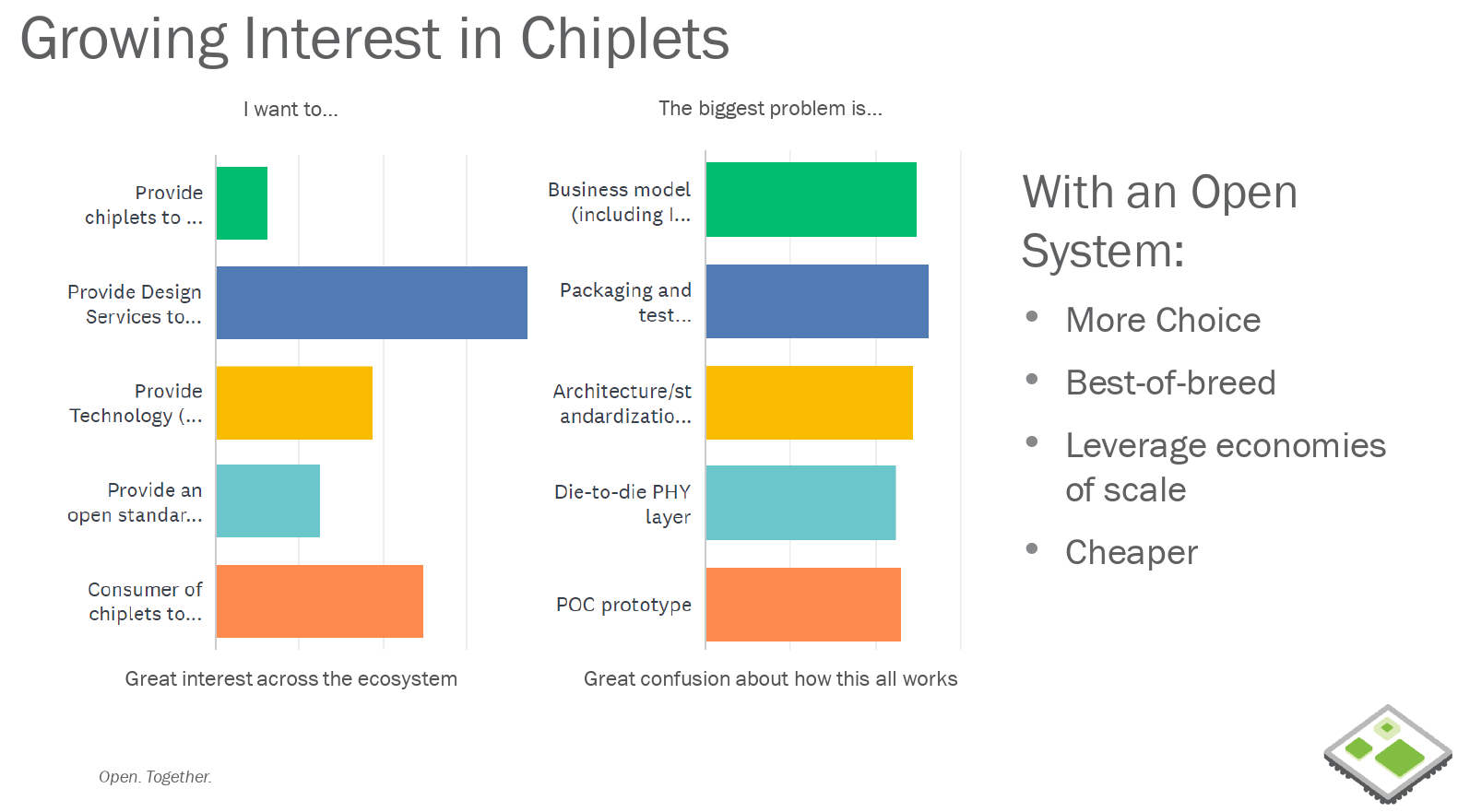
The ODSA has gained a lot of momentum since its first meeting in late 2018. From just seven original companies, close to one hundred companies have since joined. The primary interest in chiplets is the ability to lower development costs. Some companies are interested in providing niche functionalities while others are looking to acquire chiplets to build a final products. EDA tool vendors are also interested in pitching in their services. “The real problem at the moment is that no one knows how to make it all work together,†said Bapi. There are challenges that go beyond just the physical interface. Different chiplets have different functionalities. One would expect a set of limited basic functionalities to be defined as a standard from which all other functions are built on top. There are also concerns as far as packaging and testing of products across vendors. Beyond the physical implementation, there are also business issues such as pricing. Clarifying those challenges will go a long way toward enabling a coherent cross-industry open ecosystem of chiplets.
Open source collaborations are difficult in the semiconductor industry. The major showstoppers always end up around the discussion of IP sharing aspects of the design. How much IP can be shared and how much risk are they opening up to in doing so. Bill Carter, CTO of OCP, explains that such barriers become so large they often end up stagnating the project. “With the ODSA project, what we are seeing is that members are willing to see those challenges through for the industry,†said Bill.
Current Work
Although the final chips could incorporate any number of chiplets, to the outside world it should still look like a single die. To accomplish this, both physical and logical inter-die interfaces are required. By extension, for the OCP ODSA group, in order to enable a mix-and-match across the entire industry, those interfaces also have to be open interfaces.
The focus of the ODSA is developing the full architecture interface stack. This is a bit more challenging than meets the eye since the group doesn’t want to force companies into any one specific technology. It’s also unclear which technologies are winning just yet. On the physical packaging side, companies are diverging with multiple different approaches including standard organic substrates, silicon interposers, silicon bridges, as well as other options as Si-less RDL interposers. The ODSA stack is designed to be compatible with those existing technologies. This is important because it means that the OCP isn’t needlessly duplicating other active efforts such as the work being done by Intel and DARPA. Instead, they are embedding that effort into ODSA’s own efforts. In other words, chiplets designed for Intel using the AIB interface will also be OCP-compliant as well if it meets all the requirements. If you look at the full stack (shown in the slide below) you’ll see that there are multiple options at each of the layers. Diverges also exist at the PHY level. Some companies are taking the route of extending the on-die interconnects to other chiplets. Intel’s AIB and the ODSA own BoW interfaces are such examples (we will be coming back to BoW in a follow-up article). Those tend to be wide parallel buses that operate at lower data rates. Alternatively, some prefer to take off-chip serial interfaces such as PCIe and bring them on-die. On top of those interfaces, the ODSA is building a compatible network stack. Depending on the kind of chiplet being connected, there might be the need to share the memory space data. To that end, the stack includes both coherent and non-coherent data transfer protocols in order to enable the development of ‘mini open network’ between the chiplets. The full architecture interface should enable complete chiplet interoperability.
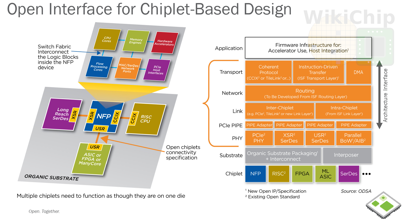
With a full-stack defined, there needs to be a means by which companies can leverage each other’s work. The OCP grand vision is a marketplace of ODSA-stack-compliant chiplets. The group wants to enable the business, tools, and workflow necessary to assemble those chiplets into finished products. It’s easy to see how from this stage on, the rest of the flow can be picked up by some of the other OCP groups. For example, the Open Accelerator Infrastructure subgroup under OCP Server Work Group has been working on a number of accelerator modules and interfaces.
Cross-industry chiplets architectures and efforts are still in its infancy. This is all work-in-progress. Undoubtedly some options will win over others. Regardless of which options win out, having open standards governed by a standards group is the only way to make a viable chiplet market become a reality.
–
Spotted an error? Help us fix it! Simply select the problematic text and press Ctrl+Enter to notify us.
–