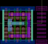
VLSI 2018: Samsung’s 8nm 8LPP, a 10nm extension
A look at Samsung’s 8nm 8LPP process that was recently disclosed at the 38th Symposium on VLSI Technology.
Read more
Your Chips and Semi News
A look at Samsung’s 8nm 8LPP process that was recently disclosed at the 38th Symposium on VLSI Technology.
Read more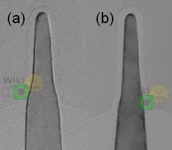
A look at Samsung’s 11nm 11LPP process that was recently disclosed at the 38th Symposium on VLSI Technology.
Read more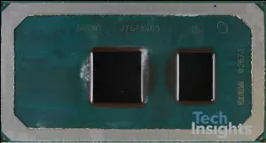
WikiChip takes another look at Intel’s 10-nanometer standard cell design and discusses TechInsights findings of the first 10nm-based chip, the i3-8121U.
Read more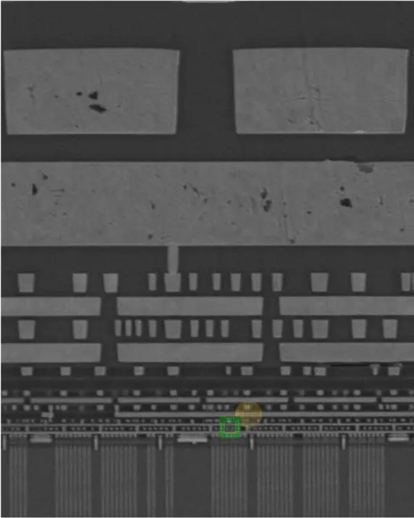
As IBM starts shipping their latest server microprocessors we take a look at the process technology that’s enabling those capabilities. Though largely thought to be the same as the original process IBM detailed back in 2014, following their fab selloff the process has undergone some unique changes making it a distinctly GlobalFoundries process now.
Read more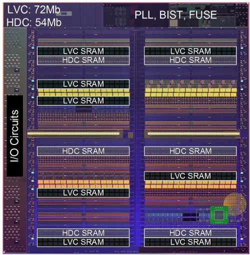
At IEDM 2017 and ISSCC 2018 Intel detailed their upcoming 10nm node, an aggressively scaled 7nm-class process technology that features new scaling accelerators as well as cobalt interconnect for the first time in high-volume manufacturing.
Read more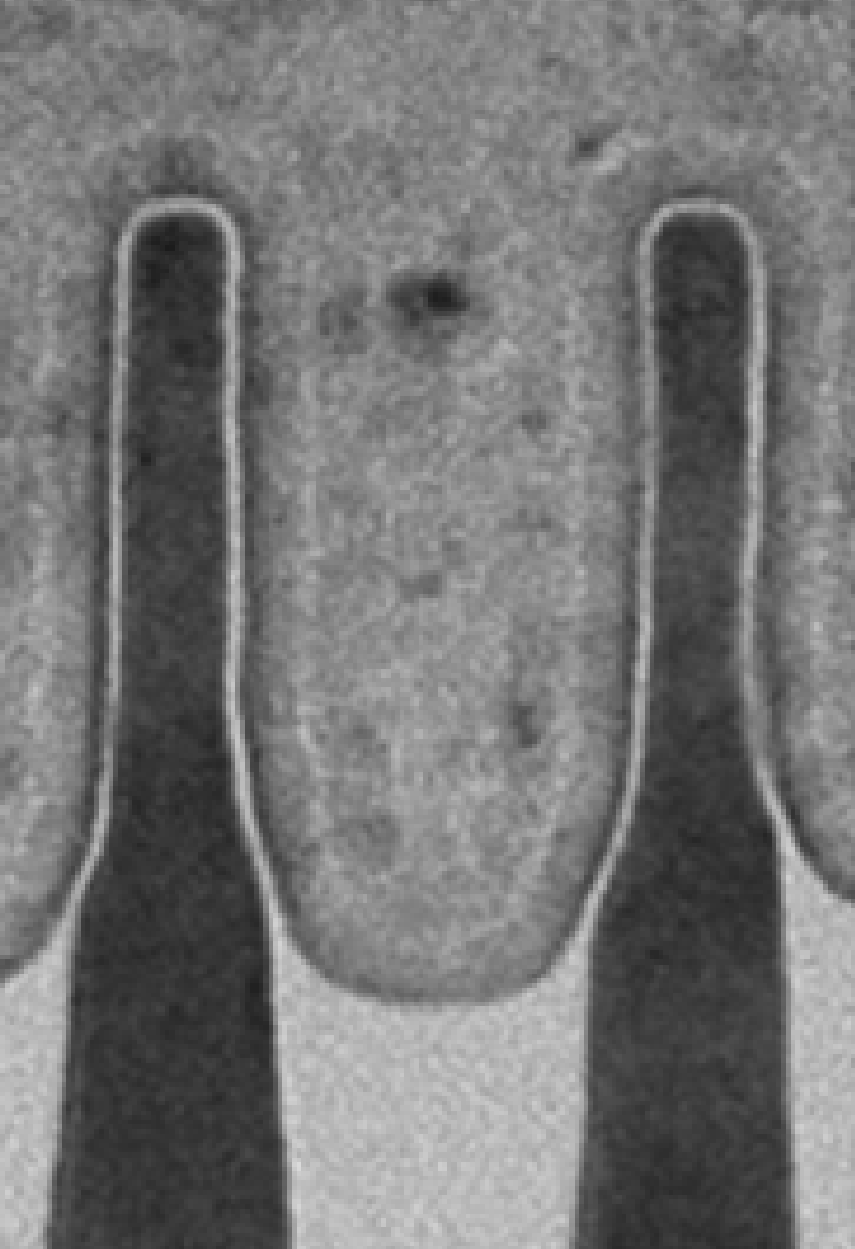
At the 2017 IEDM GlobalFoundries detailed their 7nm Leading Performance (7LP) process, an aggressively scaled version of their 14nm process optimized for next-generation mobile, SoC, and high-performance applications.
Read more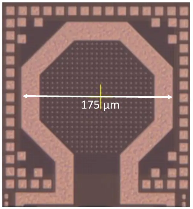
At the 2017 IEDM Intel detailed their 22FFL process, a relaxed 14nm process for Intel’s custom foundry customers. 22FFL was optimized for mobile, IoT, and RF applications offering a cost competitive process with excellent performance and simple design rules.
Read more
Samsung has announced that its 2nd generation 10nm process has entered mass production. The company also announced that their S3-Line fab in South Korea is ready to ramp up production.
Read more