
Samsung 7nm Enters Risk Production, Talks Roadmap, Scaling Boosters, and the ARM Ecosystem
3nm GAA
Samsung’s intention to switch to a new device starting with 3nm is well known. Earlier this year they announced their 3nm process a GAAFET device. This IEDM, Samsung plans to present a paper on the technology. The disclosure feels a little early but Samsung feels very confident they have a highly-manufacturable disruptive technology planned for their 3 nm and they want people to be aware of it well in advance.
Nothing is set in stone yet, but Samsung expects around 1.2x improvement in performance or up to 50% reduction in power over 7 nm. Samsung says migration from FinFET to GAA should be relatively easy. We’ll know more about their 3GGA at IEDM but one of the key benefits of GAA NSFET is the ability to vary the channel width for a variable drive like a planar transistor, breaking the FinFET restrictions of having quantized sizes. This also has interesting implications for non-logic components such as analog. PDK 0.1 will be available by next summer.
28FDS
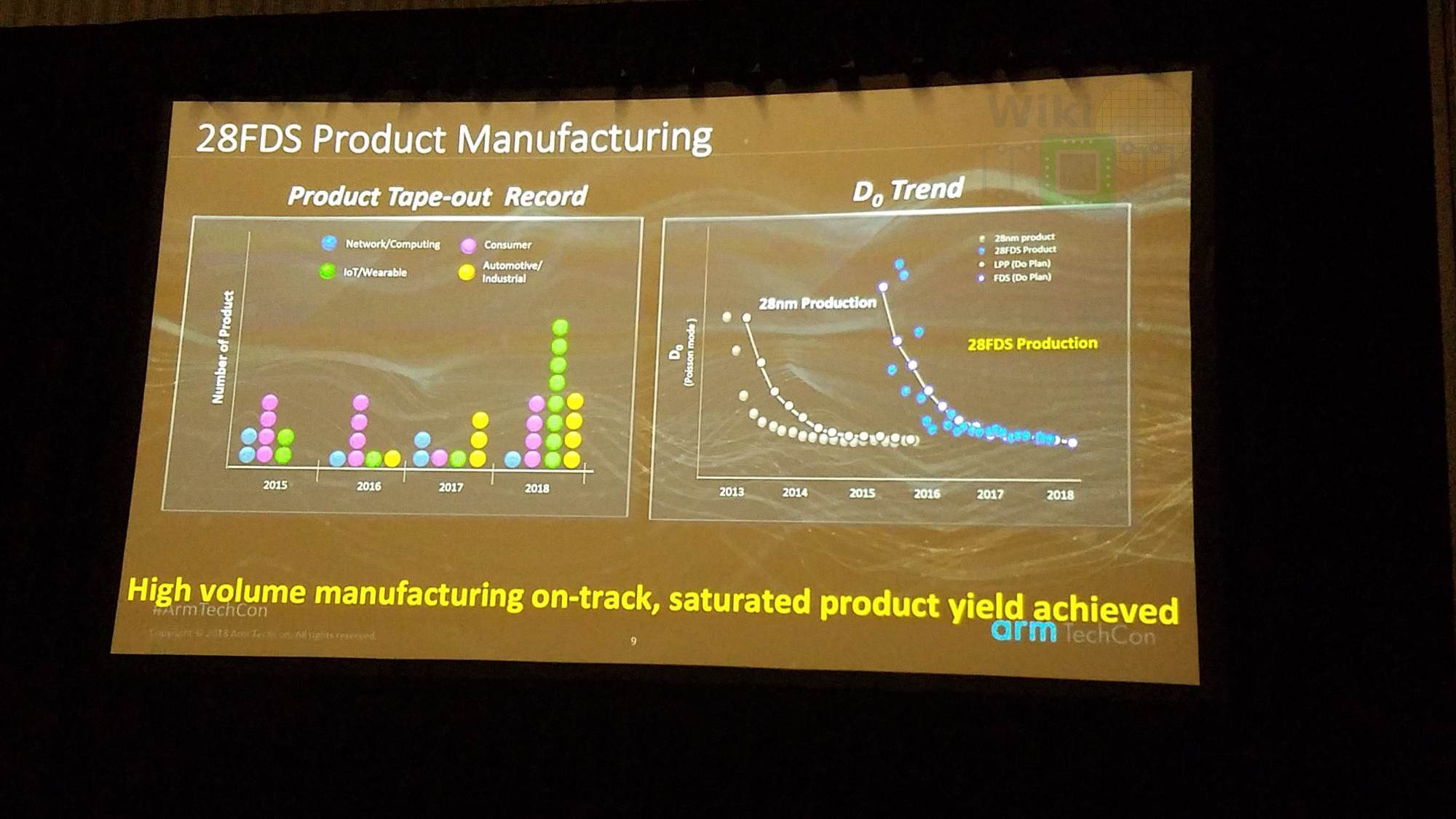
Samsung gave a short update on their 28 FD-SOI processes. The ramp was relatively fast and they are seeing a record number of tape-outs, a sign that FD-SOI might finally be gaining traction. In many ways, 28FDS no longer competes with FinFET but rather complements it in various applications. So far the company taped out 17 products with wearable/IoT leading in tape-out count. This number is expected to increase by the end of the year.
On Arm’s side, an eMRAM compiler IP for 28FDS was launched and is available starting now for use by lead partners. They have successfully completed their first eMRAM IP test chip tape out. Arm expects eMRAM to replace a large assortment of memory technologies such as Flash, EEPROM, slow SRAM, and other slow data buffers.

Packages
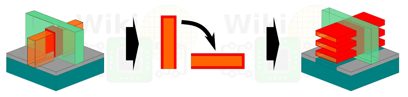
Packaging is becoming an increasingly important part of the portfolio of a leading-edge foundry. To that end, Samsung is extending their packaging portfolio to emerging AI and HPC solutions which require very large and very complex packages. Over last year, Samsung started rolling out their 2.5D silicon interposer packages with logic and HBM. In the mobile space, they have announced fan-out (FO) panel-level packaging (PLP) technology. Unlike wafer-level packaging (WLP), Samsung uses thin rectangular-shaped glass substrates they call panels on top of which they attach the die. What’s interesting is that they use the existing equipment they already use for their display technology to do this. A benefit of being rectangular is that you don’t lose out on edge placements. FO-PLP appears to already be in mass production.
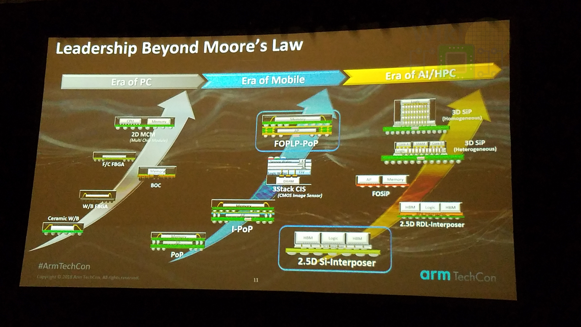
Looking forward to the next couple of years. Samsung has plans for full 3D stacked IC as well as 2.5D RDL interposer packaging. The redistribution layer (RDL) interposer can have additional components such as capacitors on it.
SAFE Ecosystem
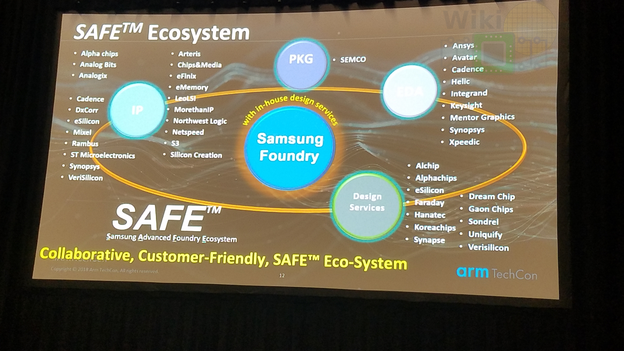
Samsung talked a little bit about own ecosystem they call Samsung Advanced Foundry Ecosystem (SAFE). Safe was announced in January 2018. At the time Samsung only had nine partners. Today, they are close to fifty. SAFE consists of four parts: IP, Packaging, EDA, and Design Services.
–
Spotted an error? Help us fix it! Simply select the problematic text and press Ctrl+Enter to notify us.
–