IEDM 2017 + ISSCC 2018: Intel’s 10nm, switching to cobalt interconnects
A Search For A Better Density Metric
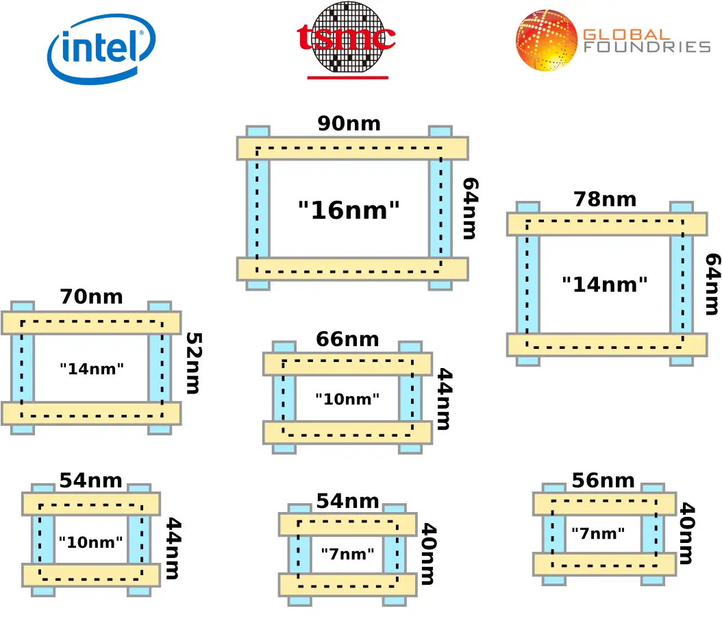
Quantifying density advantages is getting complicated. Up until very recent nodes, standard cells came in mostly similar designs. This allowed a relatively simple way of comparing densities. The oldest and perhaps still the most popular way of comparing densities is the CPPxMMx Metric. Using this method, you can simply plot the process contacted gate (poly) pitch times the metal pitch of the various processes.

Basic Geometry Is Not Enough
As transistors scaled down further with FinFET it became possible to very effectively increase drive current by increasing the fin height while reducing the pitch. With high enough drive current it became possible to perform fin depopulation – i.e. eliminating fins which enables metal tracks reduction, lowers the dynamic power, while still preserving speed or even increasing it through clever optimizations.

When foundries started reducing tracks, the old CPP x MMP Metric fell apart as it fails to capture the height of the cells that have been reduced. To compensate for this, the old metric was retrofitted to account for the difference in tracks between processes – CPP x MMP x Tracks.
Doesn’t Cover Width
As scaling continues, new innovative ways for extracting additional density is being introduced. For example COAG further reduces the cell height while using a single dummy further reduces the cell width.
| Impact On Cell Density | |
|---|---|
| Affects the Height | Affects the Width |
| Metal pitch Number of tracks COAG |
Gate pitch SDG |
Since neither the width reductions nor the height reductions can be captured by even the modified metric, Mark Bohr proposed a new metric altogether:

Supposedly it’s actually not a new metric, it simply got resurrected by Intel, albeit we’ve never heard of it. Nonetheless, the metric is a very interesting one because it successfully captures the effects of basic scaling (i.e., CPP x MMP) as well as the reduction in tracks. Additionally, since the equation relies on gate density, it also takes into account other cell optimizations that affect the cell width. The metric uses two common standard cells: 2-input NAND gate which consists of just four transistors and a fairly large scan flip-flop cell.
The total density is then a weighted sum of the average contribution of cell to the overall area. The total density consists of 60% that of the small logic cell and 40% of the complex cell.

For example, for Intel’s 10nm there are 8 diffusion lines with a fin pitch of 34nm giving us a cell height of 272. With a poly pitch is 54nm, we get [4 transistors] / [272 nm x (3 * 54 nm)] = 90.78 MTr/mm² for the NAND2 gate. For the complex flip-flop, Intel’s optimizations results in around 121 MTr/mm². The total density is thus around 102.9 MTr/mm² (note that Intel reported 100.8 MTr/mm²).
It’s worth noting that even this is insufficient to quantify the density of the process because of the cache. SRAM cells rely largely on just four metal wires: ground, power, WL, and BL. This means none of the standard density metrics can properly capture that area. What this means in practice is that a chip where the cache makes up a much larger portion of the die tends to inflate the transistor density far beyond what the MTr/mm² reports. To solve this Bohr requires that the SRAM bitcell sizes should be reported along with the MTr/mm² density value for a proper comparison.
For a discussion on how it stacks against GF’s 7nm, see the “Some Math” section here. Since large and complex logic makes up a large portion of Intel’s die, the high logic density will definitely benefit them. However, for chips with large caches, Intel is considerably behind the foundries with their solution. Overall, all the leading edge solutions are similar density-wise.
–
Spotted an error? Help us fix it! Simply select the problematic text and press Ctrl+Enter to notify us.
–
