
IBM Doubles Its 14nm eDRAM Density, Adds Hundreds of Megabytes of Cache
Late last year IBM introduced its latest Z System, the z15 mainframe. There are a number of interesting changes that were made going from z14 to z15, in this article we’ll focus on just one of those changes – the cache. The z14 has a lot of cache and the z15 even more. At the recent ISSCC conference, Christopher Berry, IBM z15 physical design team lead, presented some of the interesting changes that were made.
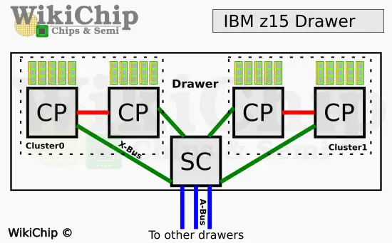
For those who are not quite familiar with the way a modern IBM mainframe is organized, you have a rack with a number of compute chassis in them called drawers. Within each drawer on the z15 are four z15 microprocessors (usually abbreviated CP for central processor). The drawer is divided into two clusters such that each CP is directly connected to the other one within the cluster. Likewise, each microprocessor is also connected to a system controller (SC) chip. There is just one SC chip in a drawer and it’s fully connected to all the other five drawers within the rack.
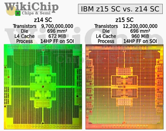
The SC chip glues the entire system together while providing a huge level 4 cache. Just how much cache are we talking about? Try 960 MiB of it in a single SC chip! That’s 43% more cache per SC over the z14. The microprocessors themselves received an equally impressive enhancement. IBM doubled the L3 cache from 128 MiB to 256 MiB. The L2 instruction cache also doubles to 4 MiB. With 12 cores on each chip, that’s 24 MiB of additional L2 instruction cache alone. Here’s the most interesting part – IBM did all that without increasing the die size by a single mm² and without changing the underlying process technology.
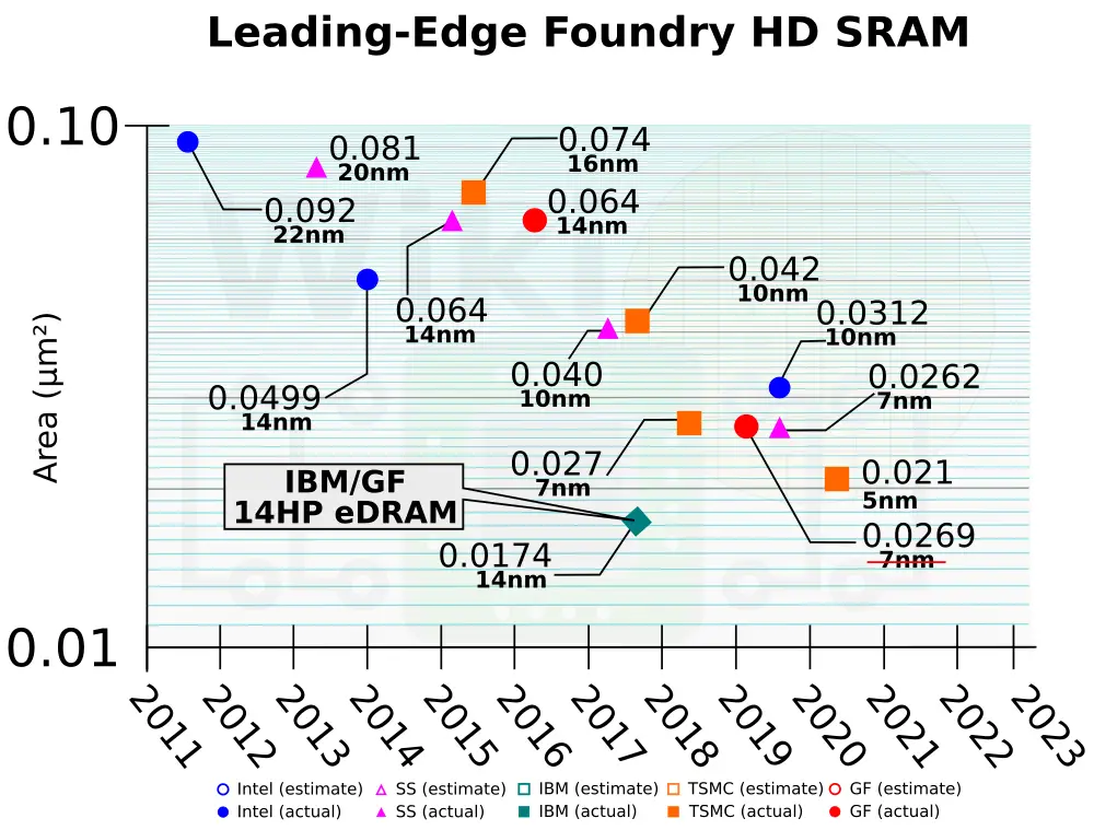
The z15, like its predecessor the z14, ended up utilizing the custom-tailor 14-nanometer FinFET on SOI process co-designed with GlobalFoundries. That process features an ultra-high-density DTC eDRAM. eDRAM has been IBM’s secret weapon for over a decade. With a single transistor along with a DTC, compared to traditional 6T cells, the density advantage is quite significant. To give you an idea of how dense it is, even on their 14 nm process, the cell size is 0.0174 μm². Currently, the densest SRAM cell reported to date on a production node is 0.021 μm² by TSMC on their yet-to-ramp 5-nanometer process. That puts IBM’s 14 nm eDRAM bit cell at about 20% denser than the densest 5 nm SRAM cell to date.
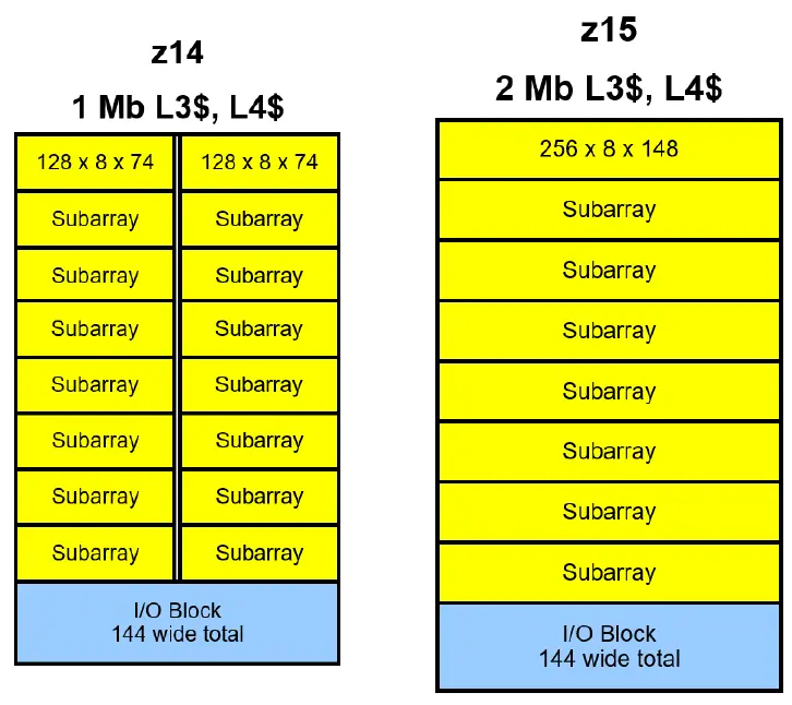
So how do you almost double the density of your eDRAM cache? It’s simple: you just ask your physical design team to do it. It turns out that by now, their 14 nm node is pretty good and there are decent overhead margins on the bitlines and wordlines. Tinkering with their z14 cells, they were able to double the bitline and wordline lengths within those margins. On their z14, the original eDRAM macro blocks for the L3 and L4 caches were a 1 MiB design consisting of sixteen sub-arrays. Each sub-array contained 128 wordlines and 592 bitlines. On the z15, they went to a 2 MiB macro design consisting of eight sub-arrays, each with 256 wordlines and 1184 bitlines.
Caches within the core (L1 and L2) operate at core frequency while caches outside of the core and at the system controller (L3 and L4) operate at half-clock. It’s worth pointing out that this change was only made to the L3 and L4 caches. Each sub-array has a sense amp shared by two groups of bitlines with each group having 128-cell bitlines. Doubling the bitline doubles the capacitance, weakening the bitline signal. To assist the line, the nFET threshold voltage was lowered and a bias voltage circuit was introduced to improve the signal margin. For the L3 and L4 caches the latency is comfortably high enough to tolerate the wordline drive strength and bitline sense impact. However, the access time required for the L2 did not allow this scheme to work. The space for the additional L2 cache was made possible through substantial physical design work within the core (will be discussed in more detail in a future article).
| z15 Caches | ||||
|---|---|---|---|---|
| Cache | L1 | L2 | L3 | L4 |
| Device | SRAM | eDRAM | eDRAM | eDRAM |
| Capacity | 128 KiB (I$) 128 KiB (D$) |
4 MiB (I$) 4 MiB (D$) |
256 MiB | 960 MiB |
| Clock | 5.2 GHz | 5.2 GHz | 2.6 GHz | 2.6 GHz |
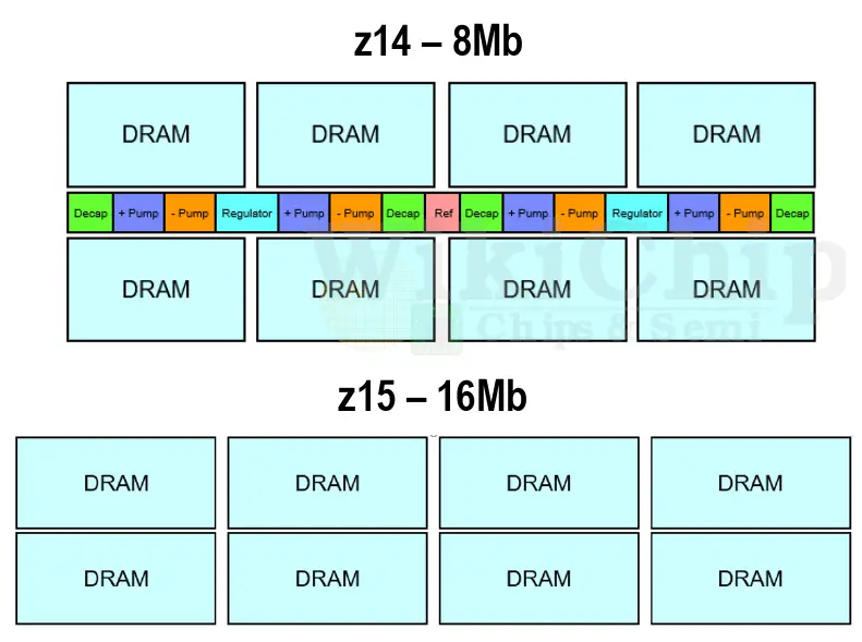
For additional space-saving, IBM altered the power delivery network of the caches. On the z14, the high-voltage generation circuit was integrated on-die. On the z15, they took those circuits off-chip and brought them back via external voltage. The low voltage generation and the regulator was brought into the macro. The generation and regulation of the low-voltage brought into the cell introduce some area and efficiency gain, however, moving the high-voltage generation circuity off-die will incur an efficiency penalty which IBM didn’t disclose.
The doubling of the bitline and wordlines and the halving of the number of sub-arrays meant quite a bit of the i/o overhead could be reduced within the array. They estimate that those modifications delivered about 30% density improvement. The power-delivery related changes produced another ~38% density improvement on top. All in all, the physical design team managed to produce a combined total effective cache density improvement of 80% (in Mib/mm²).
Related
- IBM Adds POWER9 AIO, Pushes for an Open Memory-Agnostic Interface
- IBM Introduces Next-Gen Z Mainframe: The z15; Wider Cores, More Cores, More Cache, Still 5.2 GHz
- ISSCC 2018: The IBM z14 Microprocessor And System Control Design
- POWER9 Scales Up To 1.2 TB/s of I/O, Targets NVLink 3, OpenCAPI Memory for 2019
–
Spotted an error? Help us fix it! Simply select the problematic text and press Ctrl+Enter to notify us.
–