TSMC Extends Its 5nm Family With A New Enhanced-Performance N4P Node
TSMC introduces a new 5-nanometer derivative – an enhanced performance N4P node.
Read more
Your Chips and Semi News

TSMC introduces a new 5-nanometer derivative – an enhanced performance N4P node.
Read more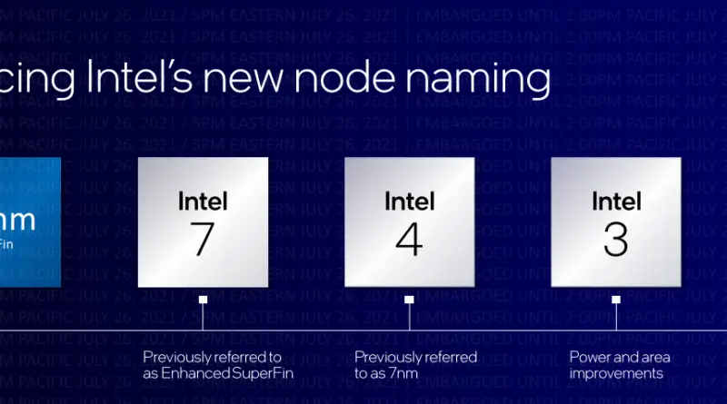
Intel 2021 Process Technology Update: Intel 7, Intel 4, Intel 3, and Intel 20A
Read more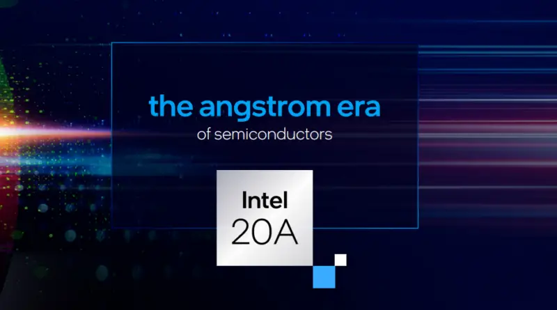
Intel announces Intel 20Å Node which will feature RibbonFET devices, PowerVia, and is set to ramp 2024.
Read more
Samsung tapes out 3nm GAA test vehicle as it inches towards mass production
Read more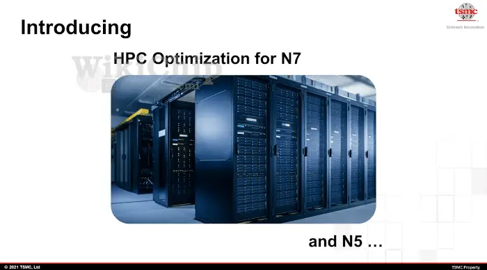
A TSMC 2021 foundry update: automotive, networking, and HPC roadmap.
Read more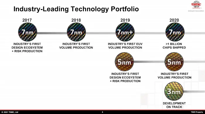
TSMC 2021 foundry update
Read more
Intel talks 10-nanometers DTCO and the benefits of EUV on their future 7 nm and 5 nm nodes.
Read more
Samsung revealed more details of its 5LPE process technology which recently ramped, gave a roadmap status update along with new stop-gap nodes announcement.
Read more
A look at the current state of leading-edge foundries for the first quarter of 2021.
Read moreTSMC announces its intention to build and operate an advanced 5-nanometer fab in Arizona.
Read more